SLVS640F October 2007 – February 2015 TPD12S520
PRODUCTION DATA.
- 1 Features
- 2 Applications
- 3 Description
- 4 Revision History
- 5 Pin Configuration and Functions
- 6 Specifications
-
7 Detailed Description
- 7.1 Overview
- 7.2 Functional Block Diagram
- 7.3
Feature Description
- 7.3.1 ±8-kV Contact ESD Protection on External Lines
- 7.3.2 Single-Chip ESD Solution for HDMI Driver
- 7.3.3 Supports All HDMI 1.3 and HDMI 1.4b Data Rates
- 7.3.4 38-Pin TSSOP Provides Seamless Layout Option With HDMI Connector
- 7.3.5 24-Pin WQFNPackage for Space Constrained Applications
- 7.3.6 Integrated Level Shifting for the Control Lines
- 7.3.7 Backdrive Protection
- 7.3.8 Lead-Free Package
- 7.4 Device Functional Modes
- 8 Application and Implementation
- 9 Power Supply Recommendations
- 10Layout
- 11Device and Documentation Support
- 12Mechanical, Packaging, and Orderable Information
パッケージ・オプション
メカニカル・データ(パッケージ|ピン)
サーマルパッド・メカニカル・データ
発注情報
7 Detailed Description
7.1 Overview
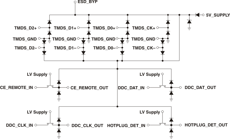
The TPD12S520 is a single-chip ESD solution for the HDMI receiver port. In many cases the core ICs, such as the scalar chipset, may not have robust ESD cells to sustain system-level ESD strikes. In these cases, the TPD12S520 provides the desired system-level ESD protection, such as the IEC61000-4-2 (Level 4) ESD, by absorbing the energy associated with the ESD strike.
While providing the ESD protection, the TPD12S520 adds little or no additional glitch in the high-speed differential signals (see Figure 7 and Figure 8). The high-speed TMDS lines add only 0.8-pF capacitance to the lines. In addition, the monolithic integrated circuit technology ensures that there is excellent matching between the two-signal pair of the differential line. This is a direct advantage over discrete ESD clamp solutions where variations between two different ESD clamps may significantly degrade the differential signal quality.
The low-speed control lines offer voltage-level shifting to eliminate the need for an external voltage level-shifter IC. The control line ESD clamps add 3.5-pF capacitance to the control lines. The 38-pin DBT package offers a seamless layout routing option to eliminate the routing glitch for the differential signal pairs. DBT package pitch (0.5 mm) matches with HDMI connector pitch. In addition, pin mapping follows the same order as the HDMI connector pin mapping. The 24-pin RMN package offers flow through routing using only two layers for highly integrated, space-efficient full HDMI protection.
7.2 Functional Block Diagram
7.3 Feature Description
7.3.1 ±8-kV Contact ESD Protection on External Lines
In many cases, the core ICs, such as the scalar chipset, may not have robust ESD cells to sustain system-level ESD strikes. In these cases, the TPD12S520 provides the desired system-level ESD protection, such as the IEC61000-4-2 (Level 4) ESD, by absorbing the energy associated with the ESD strike.
7.3.2 Single-Chip ESD Solution for HDMI Driver
TPD12S520 provides a complete ESD protection scheme for an HDMI 1.4 compliant port. The monolithic integrated circuit technology ensures that there is excellent matching between the two-signal pair of the differential line. This is a direct advantage over discrete ESD clamp solutions where variations between two different ESD clamps may significantly degrade the differential signal quality. The 38-pin DBT package offers a seamless layout routing option to eliminate the routing glitch for the differential signal pair.
7.3.3 Supports All HDMI 1.3 and HDMI 1.4b Data Rates
The high-speed TMDS pins of the TPD12S520 add only 0.8 pF of capacitance to the TMDS lines. Excellent intra-pair capacitance matching of 0.05 pF provides ultra low intra-pair skew. Insertion loss -3 dB point > 3 GHz provides enough bandwidth to pass all HDMI 1.4b TMDS data rates.
7.3.4 38-Pin TSSOP Provides Seamless Layout Option With HDMI Connector
The 38-pin DBT package offers seamless layout routing option to eliminate the routing glitch for the differential signal pair. DBT package pitch (0.5 mm) matches with HDMI connector pitch. In addition, pin mapping follows the same order as the HDMI connector pin mapping. This HDMI receiver port protection and interface device is specifically designed for next-generation HDMI receiver protection.
7.3.5 24-Pin WQFNPackage for Space Constrained Applications
The 24-pin RMN package offers flow through routing using only two layers for highly integrated, space-efficient full HDMI protection.
7.3.6 Integrated Level Shifting for the Control Lines
The low-speed control lines offer voltage-level shifting to eliminate the need for an external voltage level-shifter IC. The control line ESD clamps add 3.5-pF capacitance to the control lines.
7.3.7 Backdrive Protection
Backdrive protection is offered on the connector side pins.
7.3.8 Lead-Free Package
Lead-Free Package for RoHS Compliance.
7.4 Device Functional Modes
TPD12S520 is active with the conditions in the Recommended Operating Conditions met. The bi-directional voltage-level translators provide non-inverting level shifting from either 5V (for SDA , SCL, HPD), or 3.3 V (for CEC) on the connector side to VLV on the system side. Each connector side pin has an ESD clamp that triggers when voltages are above VBR or below the lower diode's Vf. During ESD events, voltages as high as ±8-kV (contact ESD) can be directed to ground via the internal diode network. Once the voltages on the protected line fall below these trigger levels (usually within 10's of nano-seconds), these pins revert to a non-conductive state.