SLVSA55B November 2009 – November 2016 TPD4S1394
PRODUCTION DATA.
- 1 Features
- 2 Applications
- 3 Description
- 4 Revision History
- 5 Pin Configuration and Functions
- 6 Specifications
- 7 Detailed Description
- 8 Application and Implementation
- 9 Power Supply Recommendations
- 10Layout
- 11Device and Documentation Support
- 12Mechanical, Packaging, and Orderable Information
パッケージ・オプション
メカニカル・データ(パッケージ|ピン)
- DQL|8
サーマルパッド・メカニカル・データ
- DQL|8
発注情報
8 Application and Implementation
NOTE
Information in the following applications sections is not part of the TI component specification, and TI does not warrant its accuracy or completeness. TI’s customers are responsible for determining suitability of components for their purposes. Customers should validate and test their design implementation to confirm system functionality.
8.1 Application Information
TPD4S1394 has both high-speed ESD cells to protect the D1+, D1–, D2+, and D2– lines and live insertion detection circuit to identify improper status during insertion and to control the external power switch.
8.2 Typical Application
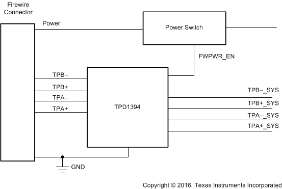
 Figure 3. Typical Application Schematic
8.2.1 Design Requirements
For this design example, a TPD4S1394 is used to protect the FireWire connector and detect live insertion.
Table 1 shows the design parameters:
Table 1. Design Parameters
| PARAMETER | EXAMPLE VALUE |
|---|---|
| Power supply, VCC | 3.3 V |
| Data line operating frequency | 400 MHz (800 Mbps) |
8.2.2 Detailed Design Procedure
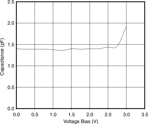
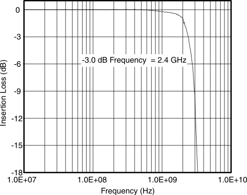
The data transfer rate of 800 Mbps is well below the bandwidth of the data pins of TPD4S1394. So the parasitics associated with the ESD cells on these lines do not degrade the signal integrity. 3.3-V power supplies are commonly available from the board and can be used to power the live insertion detection circuit.
8.2.3 Application Curves

| D+, D– Pins |

| D+, D– Pins |