SLVSBP3C December 2012 – May 2015 TPD5S116
PRODUCTION DATA.
- 1 Features
- 2 Applications
- 3 Description
- 4 Simplified Schematic
- 5 Revision History
- 6 Pin Configuration and Functions
-
7 Specifications
- 7.1 Absolute Maximum Ratings
- 7.2 ESD Ratings
- 7.3 Recommended Operating Conditions
- 7.4 Thermal Information
- 7.5 Electrical Characteristics
- 7.6 Voltage Level Shifter, SCL, SDA Lines
- 7.7 Voltage Level Shifter, CEC Line
- 7.8 Voltage Level Shifter, HPD Line
- 7.9 EN
- 7.10 Utility Pin
- 7.11 I/O Capacitances
- 7.12 Dynamic Load Characteristics
- 7.13 SCL, SDA Lines, VCCA = 1.2 V
- 7.14 CEC Line, VCCA = 1.2 V
- 7.15 HPD Line, VCCA = 1.2 V
- 7.16 SCL, SDA Lines, VCCA = 1.5 V
- 7.17 CEC Line, VCCA = 1.5 V
- 7.18 HPD Line, VCCA = 1.5 V
- 7.19 SCL, SDA Lines, VCCA = 1.8 V
- 7.20 CEC Line, VCCA = 1.8 V
- 7.21 HPD Line, VCCA = 1.8 V
- 7.22 SCL, SDA Lines, VCCA = 2.5 V
- 7.23 CEC Line, VCCA = 2.5 V
- 7.24 HPD Line, VCCA = 2.5 V
- 7.25 SCL, SDA Lines, VCCA = 3.3 V
- 7.26 CEC Line, VCCA = 3.3 V
- 7.27 HPD Line, VCCA = 3.3 V
- 7.28 SCL, SDA Lines, VCCA = 5 V
- 7.29 CEC Line, VCCA = 5 V
- 7.30 HPD Line, VCCA = 5 V
- 7.31 Typical Characteristics
-
8 Detailed Description
- 8.1 Overview
- 8.2 Functional Block Diagram
- 8.3
Feature Description
- 8.3.1 IEC 61000-4-2 Level 4 ESD Protection
- 8.3.2 Conforms to HDMI Control and 5VOUT Compliance Tests Without External Components
- 8.3.3 Auto-direction Sensing I2C Level Shifter with One-Shot Circuit to Drive Long HDMI Cable (750-pF Load)
- 8.3.4 Back Drive Protection
- 8.3.5 55-mA Load Switch with Short Circuit Protection
- 8.3.6 Hot Plug Detect Module with Pull Down Resistor
- 8.3.7 Integrated Pull-up and Pull-down Resistors per HDMI Specification
- 8.3.8 Utility Pin ESD Protection for Ethernet and Audio Return
- 8.3.9 DDC/CEC LEVEL SHIFT Circuit Operation
- 8.3.10 DDC/CEC Level Shifter Operational Notes For VCCA = 1.8V
- 8.3.11 Rise-Time Accelerators
- 8.3.12 Noise Considerations
- 8.3.13 HDMI Compliance
- 8.4 Device Functional Modes
- 9 Applications and Implementations
- 10Power Supply Requirements
- 11Layout
- 12Device and Documentation Support
- 13Mechanical, Packaging, and Orderable Information
8 Detailed Description
8.1 Overview
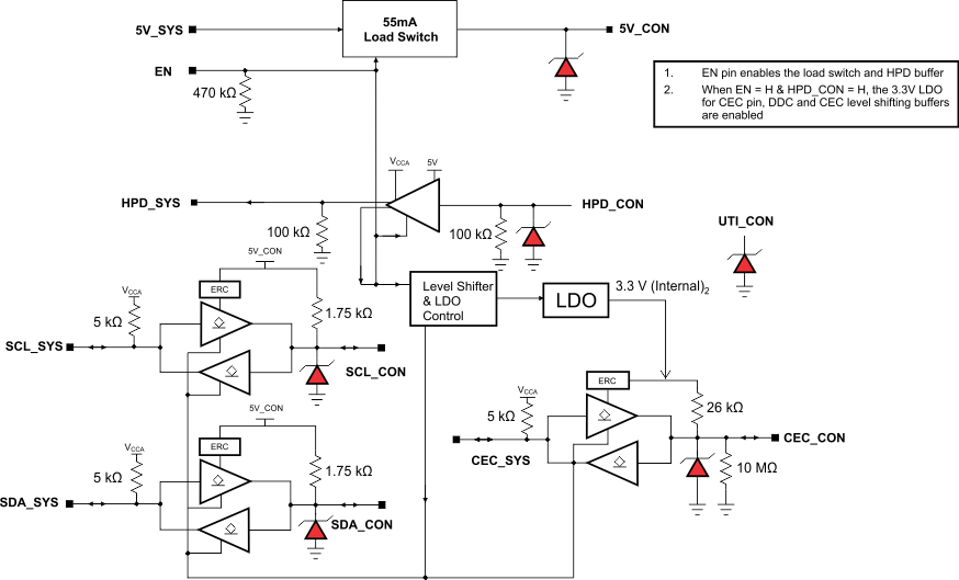
TPD5S116 is a single-chip HDMI interface electrostatic discharge (ESD) protection product with auto-direction sensing I2C voltage level shift buffers, a 5-V HDMI compliant current limited load switch, hot-plug-detect, and transient voltage suppression (TVS) with ESD protection diodes. Each connector-side pin has a TVS diode for circuit protection from ESD. The device pin mapping can be routed to either an HDMI Type D or Type C connector. An internal 3.3-V node powers the CEC pin, eliminating the need for a 3.3-V supply on board.
TPD5S116 integrates all of the external termination resistors at the HPD, CEC, SCL, and SDA lines. There are three non-inverting bidirectional translation circuits for the SDA, SCL, and CEC lines. Each has a common power rail (VCCA) on system-side from 1.1 V to 3.6V. A 55-mA current limiting switch regulates current sent from 5V_SYS to 5V_CON. The SCL and SDA pins meet the I2C specification and can drive capacitive loads greater than 750 pF, which exceeds HDMI2.0 specifications. The HPD_CON port has a glitch filter to avoid false detection due to plug bouncing during the HDMI connector insertion.
The TPD5S116 offers reverse current blocking at the 5V_CON pin. In fault conditions, such as when two HDMI transmitters are connected to the same HDMI cable, TPD5S116 ensures that the system is safe from powering up through external HDMI transmitter. The SCL_CON, SDA_CON, CEC_CON, and HPD_CON pins also feature reverse-current blocking, which ensures that the system sees no leakage if an HDMI receiver is connected while the system is powered off.
The EN pin enables the hot-plug detect and load switch. The level shifters are enabled after a valid HPD signal is detected.
8.2 Functional Block Diagram
8.3 Feature Description
8.3.1 IEC 61000-4-2 Level 4 ESD Protection
In many cases, the core ICs, such as the scalar chipset, may not have robust ESD cells to sustain system-level ESD strikes. In these cases, the TPD5S116 provides the desired system-level ESD protection, such as the IEC 61000-4-2 Level 4 ESD protection of ±15-kV Contact and Air-gap ratings by absorbing the energy associated with the ESD strike.
8.3.2 Conforms to HDMI Control and 5VOUT Compliance Tests Without External Components
The TPD5S116 is designed to be fully compliant to the HDMI 7-13 Compliance Test. See HDMI Compliance for a detailed procedure.
8.3.3 Auto-direction Sensing I2C Level Shifter with One-Shot Circuit to Drive Long HDMI Cable (750-pF Load)
The TPD5S116 contains three bidirectional open-drain buffers specifically designed to support up-translation/ down-translation between the low voltage, VCCA side DDC-bus and the 5-V DDC-bus or 3.3-V CEC line. The HDMI cable side of the DDC lines incorporates rise-time accelerators to support a high capacitive load on the HDMI cable side. The rise time accelerators boost the cable side DDC signal independent of which side of the bus is releasing the signal.
8.3.4 Back Drive Protection
The TPD5S116 offers reverse current blocking at the 5V_CON pin. In fault conditions, such as when two HDMI transmitters are connected to the same HDMI cable, TPD5S116 ensures that the system is safe from powering up through an external HDMI transmitter. The SCL_CON, SDA_CON, CEC_CON, and HPD_CON pins also feature reverse-current blocking, which ensures that the system sees no leakage if an HDMI receiver is connected while the system is powered off.
8.3.5 55-mA Load Switch with Short Circuit Protection
A 55-mA current limiting switch regulates current sent from 5V_SYS to 5V_CON. This provides protection from a short-circuit or excessive load when there is a fault condition, such as a defective HDMI cable.
8.3.6 Hot Plug Detect Module with Pull Down Resistor
Once TPD5S116 is enabled and the system’s 5-V source is on, TPD5S116 is ready for continual HDMI receiver detection. When an HDMI cable connects a receiving and transmitting device together, the 5 V on the load switch (5V_CON) flows through the receiving device’s internal resistor and into HPD’s input (HPD_CON). The HPD buffer’s output (HPD_SYS) then goes high, indicating to the transmitter that a receiving device is connected. To save power, periodic detection can be done by turning on and off the TPD5S116 before a receiving device is connected. HPD_CON port has a glitch filter to avoid false detection due to plug bouncing during the HDMI connector insertion. An integrated pull-down resistor for HPD_CON eliminates the need for an additional external component.
8.3.7 Integrated Pull-up and Pull-down Resistors per HDMI Specification
The system is designed to work properly according to the HDMI 2.0 specification with no external pull-up resistors on the DDC, CEC, and HPD lines.
8.3.8 Utility Pin ESD Protection for Ethernet and Audio Return
A TVS is provided for the Utility Pin in the HDMI connector. This pin should be routed to the TPD5S116 for proper ESD protection regardless of whether Utility is used in the application.
8.3.9 DDC/CEC LEVEL SHIFT Circuit Operation
The TPD5S116 enables DDC translation from VCCA (system-side - Port A in Figure 15) voltage levels to 5-V (HDMI connector-side - Port B in Figure 15) voltage levels without degradation of system performance. The TPD5S116 contains two bidirectional open-drain buffers specifically designed to support up-translation/down-translation between the low voltage, VCCA side DDC-bus and the 5-V DDC-bus. The connector port I/Os are over-voltage tolerant to 5.5 V, even when the device is un-powered. After power-up and with enable pin and HPD_CON pin HIGH, a LOW level on the system port (below approximately VILC = 0.08 × VCCA V) turns the connector port driver (either SDA or SCL) on and drives port B down to VOL_CON V. When the system port rises above approximately 0.10 × VCCA V, the connector port pull-down driver is turned off and the internal pull-up resistor pulls the pin HIGH. When the connector port falls first and goes below 0.3 × 5 V_CON V, a CMOS hysteresis input buffer detects the falling edge, turns on the system port driver, and pulls port A down to approximately VOLA. The connector port pull-down is not enabled unless the system port voltage goes below VILC, in which case the connector port pull-down driver is enabled until system port rises above (VILC + ΔVT-HYSTA). If the connector port is not externally driven LOW, its voltage will continue to rise due to the internal pull-up resistor.
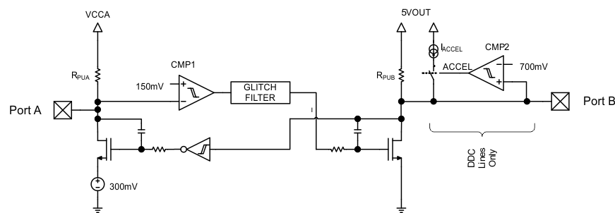 Figure 15. DDC/CEC Level Shifter Block Diagram
8.3.10 DDC/CEC Level Shifter Operational Notes For VCCA = 1.8V
- The threshold of CMP1 is ~150 mV +/- the 40mV of total hysteresis.
- The comparator will trip for a falling waveform at ~130mV
- The comparator will trip for a rising waveform at ~170mV
- To be recognized as a zero, the level at system port must first go below 130mV (VILC in spec) and then stay below 170mV (VIL_SYS in spec)
- To be recognized as a one, the level at system port must first go above 170mV and then stay above 130mV
- VILC is set to 110mV in Electrical Characteristics Table to give some margin to the 130mV
- VIL_SYS is set to 140mV in the Electrical Characteristics Table to give some margin to the 170mV
- VIH_SYS is set to 70% of VCCA to be consistent with standard CMOS levels
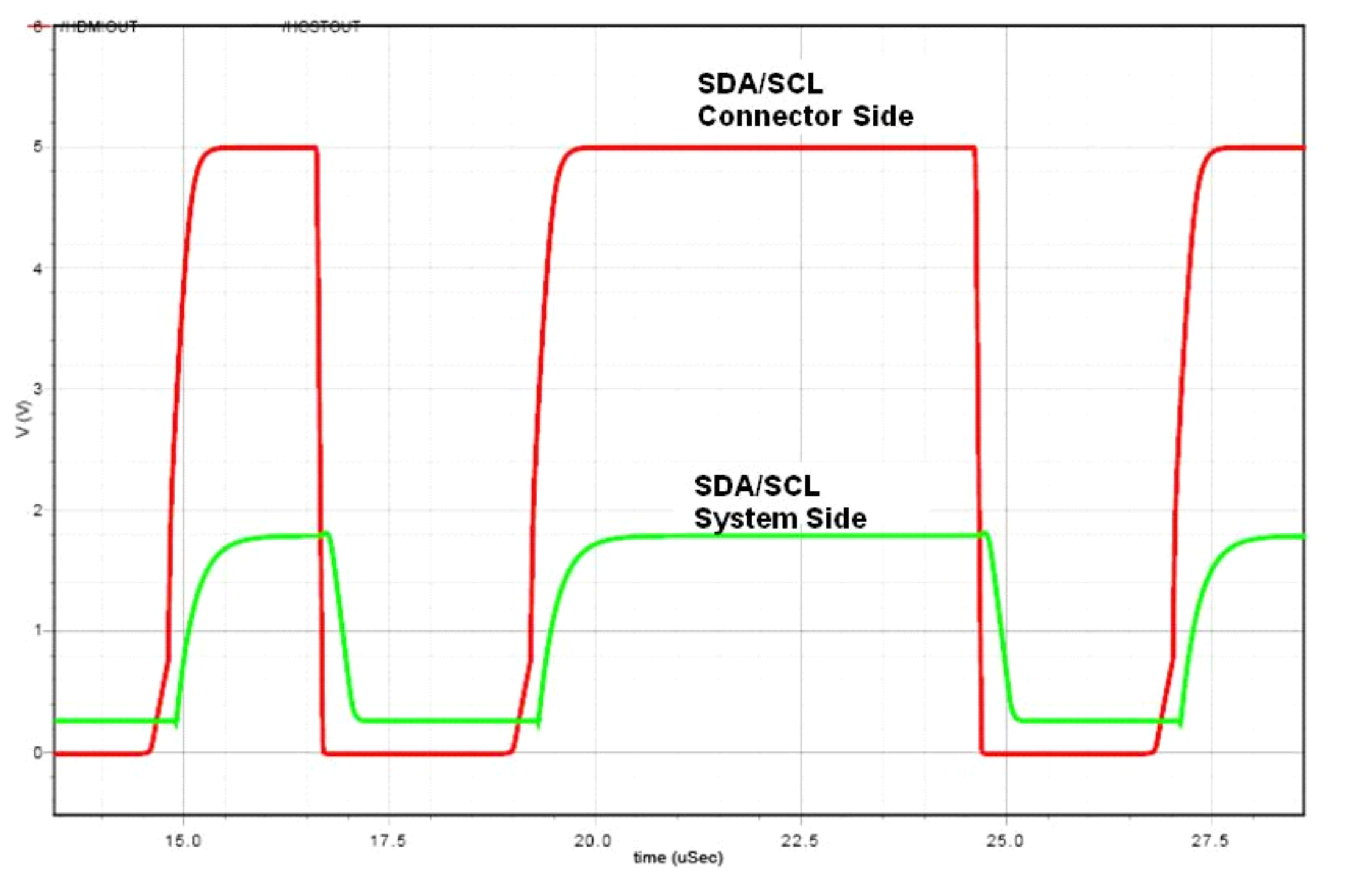 Figure 16. DDC Level Shifter Operation (Connector To System Direction)
8.3.11 Rise-Time Accelerators
The HDMI cable side of the DDC lines incorporates rise-time accelerators to support the high capacitive load on the HDMI cable side. The rise time accelerator boosts the cable side DDC signal independent of which side of the bus is releasing the signal.
8.3.12 Noise Considerations
Ground offset between the TPD5S116 ground and the ground of devices on the system port of the TPD5S116 must be avoided. The reason for this cautionary remark is that a CMOS/NMOS open-drain capable of sinking 3 mA of current at 0.4 V will have an output resistance of 133Ω or less (R = E / I). Such a driver will share enough current with the system port output pull-down of the TPD5S116 to be seen as a LOW as long as the ground offset is zero. If the ground offset is greater than 0 V, then the driver resistance must be less. Since VILC can be as low as 90 mV at cold temperatures and the low end of the current distribution, the maximum ground offset should not exceed 50 mV. Bus repeaters that use an output offset are not interoperable with the system port of the TPD5S116 as their output LOW levels will not be recognized by the TPD5S116 as a LOW. If the TPD5S116 is placed in an application where the VIL_SYS does not go below VILC, it will pull connector port LOW initially when system port input transitions LOW but the connector port will return HIGH, so it will not reproduce the system port input on connector port. Such applications should be avoided. The connector port is interoperable with all I2C-bus slaves, masters and repeaters.
8.3.13 HDMI Compliance
The TPD5S116 is designed to be fully compliant to the HDMI 7-13 capacitance specification. Both power on and power off capacitance measurements are done on the CEC, SDA, and SCL connector-side pins using a Hioki 3522-50 meter. In the power on setup, connect TPD5S116’s EN and HPD_CON pins low and 5V_SYS and VCCA pins high. Use the Hioki meter to measure the test fixture with and without the TPD5S116 and subtract to obtain the capacitance. In the power off setup, connect TPD5S116’s EN, HPD_CON, 5V_SYS, and VCCA pins low and conduct the same test with the Hioki meter. Read the Cp result from the Hioki meter.
- SCL_CON, SDA_CON Test:
- Measure the large signal capacitance at SCL_CON & SDA_CON pins at either power-up or power down conditions:
- VBIAS = 2.5 V
- f = 100 kHz
- 3.5 V p-p ac signal
- Measure the large signal capacitance at SCL_CON & SDA_CON pins at either power-up or power down conditions:
- CEC Test:
- Measure the large signal capacitance of the CEC_CON pin at both power-up and power down conditions:
- VBIAS = 1.65 V,
- f = 100 kHz
- 2.5V p-p ac signal
- Measure the large signal capacitance of the CEC_CON pin at both power-up and power down conditions:
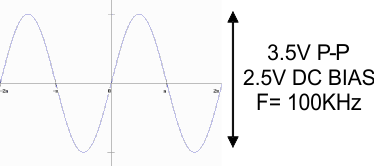 Figure 17. Hioki Meter Signal Set-Up For Scl, Sda Cap Measurement
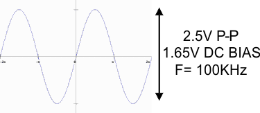 Figure 18. Hioki Meter Signal Set-Up For Cec Cap Measurement
8.4 Device Functional Modes
HDMI Driver Chip is controlling the TPD5S116 via only one control line (EN). The DDC and CEC level shifting buffers become active after HPD_CON receives a valid high signal and EN is high. EN and HPD_CON control the TPD5S116 power saving options according to the following table: