SLVS908D February 2009 – June 2015 TPS22949
PRODUCTION DATA.
- 1 Features
- 2 Applications
- 3 Description
- 4 Revision History
- 5 Description (continued)
- 6 Pin Configuration and Functions
-
7 Specifications
- 7.1 Absolute Maximum Ratings
- 7.2 ESD Ratings
- 7.3 Recommended Operating Conditions
- 7.4 Thermal Information
- 7.5 Electrical Characteristics
- 7.6 Current Limiter Electrical Characteristics
- 7.7 Low-Noise LDO Regulator Electrical Characteristics
- 7.8 Current Limiter Switching Characteristics
- 7.9 Typical Characteristics
- 8 Detailed Description
- 9 Application and Implementation
- 10Power Supply Recommendations
- 11Layout
- 12Device and Documentation Support
- 13Mechanical, Packaging, and Orderable Information
パッケージ・オプション
メカニカル・データ(パッケージ|ピン)
- DRG|8
サーマルパッド・メカニカル・データ
- DRG|8
発注情報
8 Detailed Description
8.1 Overview
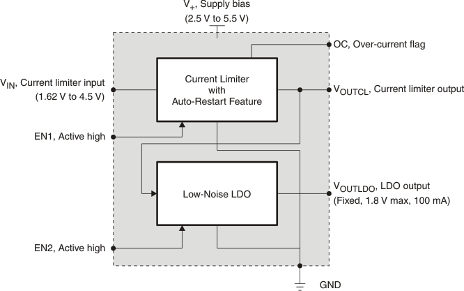
The TPS22949 and TPS22949A are devices that provide protection to systems and loads in high-current conditions. The device contains a 500-mΩ current-limited P-channel MOSFET that can operate over an input voltage range of 1.62 V to 4.5 V. In addition, these devices feature a low-dropout regulator (LDO) with a fixed output voltage of 1.8 V. When the switch current reaches the maximum limit, the TPS22949/TPS22949A operates in a constant-current mode to prohibit excessive currents from causing damage. The fault signal pin (OC) will signal the constant current condition if it persists after 12 ms. The output of the current limiter is internally connected to the LDO.
8.2 Functional Block Diagram
 Figure 41. Simplified Block Diagram
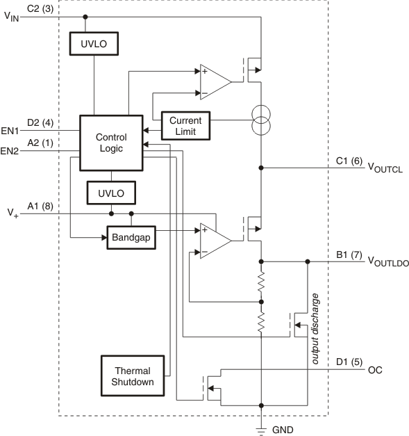
 Figure 42. Detailed Block Diagram
8.3 Feature Description
8.3.1 Undervoltage Lockout (UVLO)
The undervoltage lockout turns off the switch if the input voltage drops below the undervoltage lockout threshold. With the ON pin active, the input voltage rising above the undervoltage lockout threshold causes a controlled turnon of the switch, which limits current overshoots. The TPS22949 and TPS22949A also have a UVLO on the V+ bias voltage and keep the output of the LDO shut off until the internal circuitry is operating properly.
8.3.2 Fault Reporting
When an overcurrent, input undervoltage, or overtemperature condition is detected, OC is set active low to signal the fault mode. OC is an open-drain MOSFET and requires a pullup resistor between VIN and OC. During shutdown, the pulldown on OC is disabled, thus reducing current draw from the supply.
8.3.3 Current Limiting
When the switch current reaches the maximum limit, the TPS22949/TPS22949A operates in a constant-current mode to prohibit excessive currents from causing damage. TPS22949/TPS22949A has a minimum current limit of 100 mA.
8.4 Device Functional Modes
Table 1 summarizes the LDO state as determined by the EN1 and EN2 pins.
Table 1. Function Table
| STATE OF THE DEVICE | EN1 | EN2 |
|---|---|---|
| Current limiter and LDO disabled | 0 | X |
| Current limiter enabled and LDO disabled | 1 | 0 |
| Current limiter and LDO enabled | 1 | 1 |