SLVS788D February 2009 – November 2016 TPS22951
PRODUCTION DATA.
- 1 Features
- 2 Applications
- 3 Description
- 4 Revision History
- 5 Pin Configurations and Functions
- 6 Specifications
- 7 Parameter Measurement Information
- 8 Detailed Description
- 9 Application and Implementation
- 10Power Supply Recommendations
- 11Layout
- 12Device and Documentation Support
- 13Mechanical, Packaging, and Orderable Information
9 Application and Implementation
NOTE
Information in the following applications sections is not part of the TI component specification, and TI does not warrant its accuracy or completeness. TI’s customers are responsible for determining suitability of components for their purposes. Customers should validate and test their design implementation to confirm system functionality.
9.1 Application Information
The input to output voltage drop in the device is determined by the RON of the device and the load current. The RON of the device depends upon the VCC condition of the device. Refer to Figure 1 rON vs VCC to determine the rON of the device based upon the VCC condition. Use Equation 1 to calculate the input to output voltage drop:

where
- ΔV = voltage drop from VCC to PWR
- ILOAD = load current
- RON = ON-Resistance of the device for a specific VCC
9.2 Typical Application
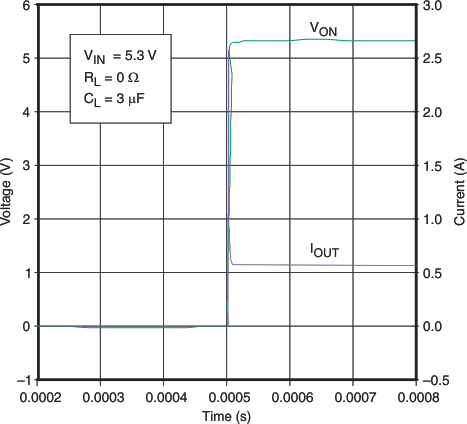
This application demonstrates how the TPS22951 can be used to protect against a short-circuit event. In this application, the PWR node is accidentally shorted to ground.
 Figure 12. Typical Application Circuit
9.2.1 Design Requirements
For this design example, use the input parameters given in Table 2:
Table 2. Design Parameters
| DESIGN PARAMTER | EXAMPLE VALUE |
|---|---|
| Power Supply Maximum DC Output Current | 2 A |
| Load 1 Current Consumption | 1 A |
9.2.2 Detailed Design Procedure
The power supply provides power to multiple loads. In the event that Load 2 is shorted to ground, the power supply must continue providing power to Load 1. The power supply can provide 2-A continuous current. Load 1 consumes 1-A continuous current. The TPS22951 is used to ensure that Load 2 consumes less than 1-A continuous current. This ensures that the power supply can provide power to Load 1 even in the case that Load 2 is shorted to ground.
9.2.3 Application Curve
 Figure 13. Device Enabled into Short-Circuit