SLVSAL2G January 2011 – November 2015 TPS24710 , TPS24711 , TPS24712 , TPS24713
PRODUCTION DATA.
- 1 Features
- 2 Applications
- 3 Description
- 4 Revision History
- 5 Device Comparison Table
- 6 Pin Configuration and Functions
- 7 Specifications
- 8 Detailed Description
-
9 Application and Implementation
- 9.1 Application Information
- 9.2
Typical Application
- 9.2.1 Design Requirements
- 9.2.2
Detailed Design Procedure
- 9.2.2.1
Power-Limited Start-Up
- 9.2.2.1.1 STEP 1. Choose RSENSE
- 9.2.2.1.2 STEP 2. Choose MOSFET M1
- 9.2.2.1.3 STEP 3. Choose Power-Limit Value, PLIM, and RPROG
- 9.2.2.1.4 STEP 4. Choose Output Voltage Rising Time, tON, CT
- 9.2.2.1.5 STEP 5. Calculate the Retry-Mode Duty Ratio
- 9.2.2.1.6 STEP 6. Select R1 and R2 for UV
- 9.2.2.1.7 STEP 7. Choose RGATE, R4, R5 and C1
- 9.2.2.2 Additional Design Considerations
- 9.2.2.1
Power-Limited Start-Up
- 9.2.3 Application Curve
- 10Power Supply Recommendations
- 11Layout
- 12Device and Documentation Support
- 13Mechanical, Packaging, and Orderable Information
11 Layout
11.1 Layout Guidelines
TPS24710/11/12/13 applications require careful attention to layout to ensure proper performance and to minimize susceptibility to transients and noise. In general, all traces should be as short as possible, but the following list deserves first consideration:
- Decoupling capacitors on VCC pin should have minimal trace lengths to the pin and to GND.
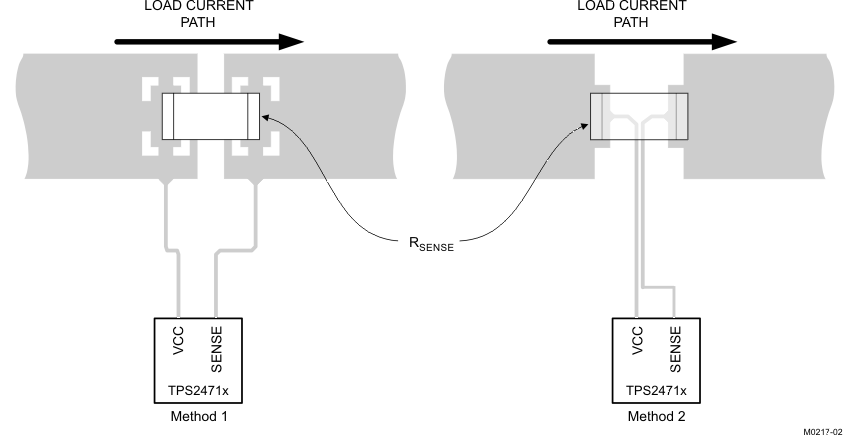
- Traces to VCC and SENSE must be short and run side-by-side to maximize common-mode rejection. Kelvin connections should be used at the points of contact with RSENSE. (see Figure 39).
- Power path connections should be as short as possible and sized to carry at least twice the full load current, more if possible.
- Protection devices such as snubbers, TVS, capacitors, or diodes should be placed physically close to the device they are intended to protect, and routed with short traces to reduce inductance. For example, the protection Schottky diode shown in the typical application diagram on the front page of this data sheet should be physically close to the OUT pin.
11.2 Layout Example
 Figure 39. Recommended RSENSE Layout