JAJSHQ7A July   2019  – September 2019 TPS3870-Q1

PRODUCTION DATA.  

  1. 特長
  2. アプリケーション
  3. 概要
    1.     Device Images
      1.      過電圧検出機能を内蔵
      2.      過電圧精度の標準的な分散
  4. 改訂履歴
  5. 概要(続き)
  6. Device Comparison Table
  7. Pin Configuration and Functions
    1.     Pin Functions
  8. Specifications
    1. 8.1 Absolute Maximum Ratings
    2. 8.2 ESD ratings
    3. 8.3 Recommended Operating Conditions
    4. 8.4 Thermal Information
    5. 8.5 Electrical Characteristics
    6. 8.6 Timing Requirements
    7. 8.7 Typical Characteristics
  9. Detailed Description
    1. 9.1 Overview
    2. 9.2 Functional Block Diagram
    3. 9.3 Feature Description
      1. 9.3.1 VDD
      2. 9.3.2 SENSE
      3. 9.3.3 RESET
      4. 9.3.4 Capacitor Time (CT)
      5. 9.3.5 Manual Reset (MR)
    4. 9.4 Device Functional Modes
      1. 9.4.1 Normal Operation (VDD > VDD(MIN))
      2. 9.4.2 Undervoltage Lockout (VPOR < VDD < UVLO)
      3. 9.4.3 Power-On Reset (VDD < VPOR)
  10. 10Application and Implementation
    1. 10.1 Application Information
      1. 10.1.1 Voltage Threshold Accuracy
      2. 10.1.2 CT Reset Time Delay
        1. 10.1.2.1 Factory-Programmed Reset Delay Timing
        2. 10.1.2.2 Programmable Reset Delay-Timing
      3. 10.1.3 RESET Latch Mode
      4. 10.1.4 Adjustable Voltage Thresholds
      5. 10.1.5 Immunity to SENSE Pin Voltage Transients
        1. 10.1.5.1 Hysteresis
    2. 10.2 Typical Application
      1. 10.2.1 Design 1: RESET Latch Mode
        1. 10.2.1.1 Design Requirements
        2. 10.2.1.2 Detailed Design Procedure
        3. 10.2.1.3 Application Curves
  11. 11Power Supply Recommendations
    1. 11.1 Power Supply Guidelines
  12. 12Layout
    1. 12.1 Layout Guidelines
    2. 12.2 Layout Example
  13. 13デバイスおよびドキュメントのサポート
    1. 13.1 デバイスの項目表記
    2. 13.2 ドキュメントのサポート
      1. 13.2.1 評価基板
    3. 13.3 ドキュメントの更新通知を受け取る方法
    4. 13.4 サポート・リソース
    5. 13.5 商標
    6. 13.6 静電気放電に関する注意事項
    7. 13.7 Glossary
  14. 14メカニカル、パッケージ、および注文情報

パッケージ・オプション

メカニカル・データ(パッケージ|ピン)
サーマルパッド・メカニカル・データ
発注情報

Pin Configuration and Functions

DSE Package
6-Pin WSON
Top View
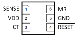
TPS3870-Q1 DSE-6-Package-Drawing.gif

Pin Functions

PIN I/O DESCRIPTION
NO. NAME
1 SENSE I Input for the monitored supply voltage rail. When the SENSE voltage goes above the overvoltage threshold, the RESET pin is driven low. Connect to VDD pin if monitoring VDD supply voltage.
2 VDD I Supply voltage input pin. Good analog design practice is to place a 0.1-μF ceramic capacitor close to this pin.
3 CT I Capacitor time delay pin. The CT pin offers two fixed time delays by connecting CT pin to VDD or leaving it floating. Delay time can be programmed by connecting an external capacitor reference to ground.
4 RESET O Active-low, open-drain output. This pin goes low when the SENSE voltage rises above the internally overvoltage threshold (VIT+). See the timing diagram in Figure 19 for more details. Connect this pin to a pull-up resistor terminated to the desired pull-up voltage.
5 GND Ground
6 MR I Manual reset (MR), pull this pin to a logic low (VMR_L) to assert a reset signal . After the MR pin is deasserted the output goes high after the reset delay time(tD) expires. MR can be left floating when not in use.