JAJSHK0B NOVEMBER 2008 – June 2019 TPS40197
PRODUCTION DATA.
- 1 特長
- 2 アプリケーション
- 3 概要
- 4 改訂履歴
- 5 概要(続き)
- 6 Pin Configuration and Functions
- 7 Specifications
- 8 Detailed Description
- 9 Application and Implementation
- 10デバイスおよびドキュメントのサポート
- 11メカニカル、パッケージ、および注文情報
パッケージ・オプション
メカニカル・データ(パッケージ|ピン)
- RGY|16
サーマルパッド・メカニカル・データ
- RGY|16
発注情報
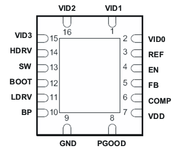
6 Pin Configuration and Functions
RGY Package
16-Pin VQFN
Top View

Pin Functions
| PIN | I/O | DESCRIPTION | |
|---|---|---|---|
| NAME | NO. | ||
| BOOT | 12 | I | Gate drive voltage for the high-side N-channel MOSFET. A 100-nF capacitor (typical) must be connected between this pin and SW. |
| BP | 10 | O | Output bypass for the internal regulator. Connect a low ESR bypass ceramic capacitor of 1 μF or greater from this pin to GND. |
| COMP | 6 | O | Output of the error amplifier and connection node for loop feedback components. |
| EN | 4 | I | Logic level input which starts or stops the controller from an external user command. A high level turns the controller on. A weak internal pullup holds this pin high so that the pin may be left floating if this function is not used. Pulling this pin low disables the controller. |
| FB | 5 | I | Inverting input to the error amplifier. |
| HDRV | 14 | O | Bootstrapped gate drive output for the high-side N-channel MOSFET. |
| LDRV | 11 | O | Gate drive output for the low-side synchronous rectifier N-channel MOSFET. |
| PGOOD | 8 | O | Open drain power good output. |
| REF | 3 | I | Non-Inverting input to the error amplifier. Its voltage range is from 0.9 V to 1.2 V in 20-mV steps. It is also internally connected to the DAC output through a unit gain buffer with 650-μA source/sink current capability. An external capacitor connected from this pin to GND programs the output voltage transition rate when VID code changes. |
| VDD | 7 | I | Power input to the controller. Connect a 1-μF bypass capacitor closely from this pin to GND. |
| VID0 | 2 | I | Logic level inputs to the internal DAC that provides the reference voltage for output regulation. These pins are internally pulled up to a 1.68-V source with 80-μA pullup current. |
| VID1 | 1 | I | |
| VID2 | 16 | I | |
| VID3 | 15 | I | |
| GND | 9 | Ground connection to the controller | |