SLUS600E April 2004 – December 2014 TPS51100
PRODUCTION DATA.
10 Layout
10.1 Layout Guidelines
Consider the following points before the layout of TPS51100 design begins.
- The input bypass capacitor for VLDOIN should be placed to the pin as close as possible with a short and wide connection.
- The output capacitor for VTT should be placed close to the pin with a short and wide connection in order to avoid additional ESR and/or ESL of the trace.
- VTTSNS should be connected to the positive node of VTT output capacitor(s) as a separate trace from the high current power line and is strongly recommended to avoid additional ESR and/or ESL. If it is needed to sense the voltage of the point of the load, it is recommended to attach the output capacitor(s) at that point. Also, it is recommended to minimize any additional ESR and/or ESL of the ground trace between the GND pin and the output capacitor(s).
- Consider adding an LPF at VTTSNS in case the ESR of the VTT output capacitor(s) is larger than 2 mΩ.
- VDDQSNS can be connected separately from VLDOIN. Remember that this sensing potential is the reference voltage of VTTREF. Avoid any noise generative lines.
- The negative node of the VTT output capacitor(s) and the VTTREF capacitor should be tied together, avoiding common impedance to the high-current path of the VTT source/sink current.
- The GND (signal GND) pin node represents the reference potential for the VTTREF and VTT outputs. Connect GND to the negative nodes of the VTT capacitor(s), VTTREF capacitor, and VDDQ capacitor(s) with care to avoid additional ESR and/or ESL. GND and PGND (Power GND) should be isolated, with a single point connection between them.
- In order to remove heat from the package effectively, prepare the thermal land and solder to the package thermal pad. The wide trace of the component-side copper, connected to this thermal land, helps heat spreading. Numerous vias 0.33 mm in diameter connected from the thermal land to the internal/solder-side ground plane(s) should be used to help dissipation.
10.2 Layout Example
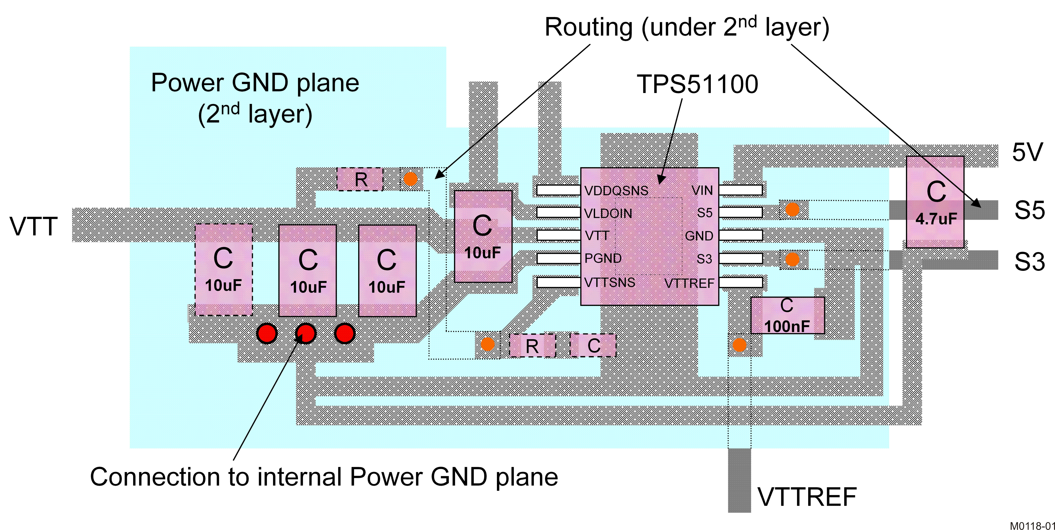
2. The negative terminal of each output capacitor should be directly connected to GND of the IC; do not use a VIA.
3. VIAs
 VIA between 1st and 2nd layers
 VIA between 1st and other layers under 2nd
4. Rs and Cs with dotted outlines are options.
10.3 Thermal Considerations
As the TPS51100 is a linear regulator, the VTT current flow in both source and sink directions generates power dissipation from the device. In the source phase, the potential difference between VVLDOIN and VVTT times VTT current becomes the power dissipation, WDSRC.
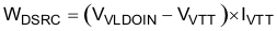
In this case, if VLDOIN is connected to an alternative power supply lower than VDDQ voltage, power loss can be decreased.
For the sink phase, VTT voltage is applied across the internal LDO regulator, and the power dissipation, and WDSNK, is calculated by:
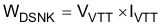
Because the device does not sink and source the current at the same time and IVTT varies rapidly with time, the actual power dissipation that must be considered for thermal design is an average over the thermal relaxation duration of the system. Another power consumption is the current used for internal control circuitry from the VIN supply and VLDOIN supply. This can be estimated as 20 mW or less at normal operational conditions. This power must be effectively dissipated from the package. Maximum power dissipation allowed to the package is calculated by,
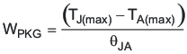
where
TJ(max) is 125°C
TA(max) is the maximum ambient temperature in the system
θJA is the thermal resistance from the silicon junction to the ambient
This thermal resistance strongly depends on the board layout. TPS51100 is assembled in a thermally enhanced PowerPAD package that has an exposed die pad underneath the body. For improved thermal performance, this die pad must be attached to the ground trace via thermal land on the PCB. This ground trace acts as a heat sink/spread. The typical thermal resistance, 57.7°C/W, is achieved based on a 3 mm × 2 mm thermal land with two vias without air flow. It can be improved by using larger thermal land and/or increasing the number of vias. For example, assuming a 3 mm × 3 mm thermal land with four vias without air flow, it is 45.4°C/W. Further information about the PowerPAD package and its recommended board layout is described in the PowerPAD Thermally Enhanced Package application report (SLMA002). This document is available at www.ti.com.