SLVSCT3 March 2015 TPS51275B-1
PRODUCTION DATA.
- 1 Features
- 2 Applications
- 3 Description
- 4 Typical Application Diagram
- 5 Revision History
- 6 Pin Configuration and Functions
- 7 Specifications
-
8 Detailed Description
- 8.1 Overview
- 8.2 Functional Block Diagram
- 8.3
Feature Description
- 8.3.1 PWM Operations
- 8.3.2 Adaptive On-Time and PWM Frequency Control
- 8.3.3 Light-Load Condition in Out-of-Audio Operation
- 8.3.4 Enable and Power Good
- 8.3.5 Soft-Start and Discharge
- 8.3.6 VREG5 and VREG3 Linear Regulators
- 8.3.7 VCLK for Charge Pump
- 8.3.8 Overcurrent Protection
- 8.3.9 Output Overvoltage and Undervoltage Protection
- 8.3.10 Undervoltage Lockout Protection
- 8.3.11 Over-Temperature Protection (OTP)
- 8.4 Device Functional Modes
- 9 Application and Implementation
- 10Power Supply Recommendations
- 11Layout
- 12Device and Documentation Support
- 13Mechanical, Packaging, and Orderable Information
パッケージ・オプション
メカニカル・データ(パッケージ|ピン)
- RUK|20
サーマルパッド・メカニカル・データ
- RUK|20
発注情報
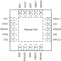
6 Pin Configuration and Functions
RUK Package
20-Pin WQFN With Thermal Pad
Top View

Pin Functions
| PIN | I/O | DESCRIPTION | |
|---|---|---|---|
| NAME | NO. | ||
| CS1 | 1 | O | Sets the channel 1 OCL trip level |
| CS2 | 5 | O | Sets the channel 2OCL trip level |
| DRVH1 | 16 | O | High-side driver output |
| DRVH2 | 10 | O | High-side driver output |
| DRVL1 | 15 | O | Low-side driver output |
| DRVL2 | 11 | O | Low-side driver output |
| EN1 | 20 | I | Channel 1 enable |
| EN2 | 6 | I | Channel 2 enable |
| PGOOD | 7 | O | Power good output flag. Open drain output. Pull up to external rail through a resistor |
| SW1 | 18 | O | Switch-node connection |
| SW2 | 8 | O | Switch-node connection |
| VBST1 | 17 | I | Supply input for high-side MOSFET (bootstrap terminal). Connect a capacitor from this pin to the SWx pin. |
| VBST2 | 9 | I | |
| VCLK | 19 | O | Clock output for charge pump |
| VFB1 | 2 | I | Voltage feedback input |
| VFB2 | 4 | I | |
| VIN | 12 | I | Power conversion voltage input. Apply the same voltage as drain voltage of high-side MOSFETs of channel 1 and channel 2. |
| VO1 | 14 | I | Output voltage input, 5-V input for switch-over |
| VREG3 | 3 | O | 3.3-V LDO output |
| VREG5 | 13 | O | 5-V LDO output |
| Thermal pad | — | Ground (GND) terminal, solder to the ground plane | |