JAJSGR0F December 2010 – December 2018 TPS51916
PRODUCTION DATA.
- 1 特長
- 2 アプリケーション
- 3 概要
- 4 改訂履歴
- 5 概要(続き)
- 6 Pin Configuration and Functions
- 7 Specifications
-
8 Detailed Description
- 8.1 Overview
- 8.2 Functional Block Diagram
- 8.3
Feature Description
- 8.3.1 VDDQ Switch Mode Power Supply Control
- 8.3.2 VREF and REFIN, VDDQ Output Voltage
- 8.3.3 Soft-Start and Powergood
- 8.3.4 Power State Control
- 8.3.5 Discharge Control
- 8.3.6 VTT and VTTREF
- 8.3.7 VDDQ Overvoltage and Undervoltage Protection
- 8.3.8 VDDQ Out-of-Bound Operation
- 8.3.9 VDDQ Overcurrent Protection
- 8.3.10 VTT Overcurrent Protection
- 8.3.11 V5IN Undervoltage Lockout Protection
- 8.3.12 Thermal Shutdown
- 8.4 Device Functional Modes
- 8.5 D-CAP2™ Mode Operation
- 9 Application and Implementation
- 10Power Supply Recommendations
- 11Layout
- 12デバイスおよびドキュメントのサポート
- 13メカニカル、パッケージ、および注文情報
8.3.3 Soft-Start and Powergood
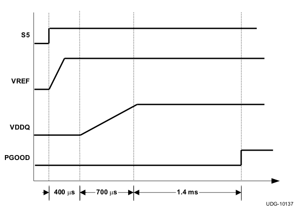
Provide a voltage supply to VIN and V5IN before asserting S5 to high. TPS51916 device provides integrated VDDQ soft-start functions to suppress in-rush current at start-up. The soft-start is achieved by controlling internal reference voltage ramping up. Figure 34 shows the start-up waveforms. The switching regulator waits for 400μs after S5 assertion. The MODE pin voltage is read in this period. A typical VDDQ ramp up duration is 700μs.
TPS51916 device has a powergood open-drain output that indicates the VDDQ voltage is within the target range. The target voltage window and transition delay times of the PGOOD comparator are ±8% (typ) and 1-ms delay for assertion (low to high), and ±16% (typ) and 330-ns delay for de-assertion (high to low) during running. The PGOOD start-up delay is 2.5 ms after S5 is asserted to high. Note that the time constant which is composed of the REFIN capacitor and a resistor divider needs to be short enough to reach the target value before PGOOD comparator enabled.
 Figure 34. Typical Start-up Waveforms