JAJSBU2G August 2011 – April 2021 TPS53355
PRODUCTION DATA
- 1 特長
- 2 アプリケーション
- 3 概要
- 4 Revision History
- 5 Pin Configuration and Functions
- 6 Specifications
-
7 Detailed Description
- 7.1 Overview
- 7.2 Functional Block Diagram
- 7.3
Feature Description
- 7.3.1 5-V LDO and VREG Start-Up
- 7.3.2 Adaptive On-Time D-CAP Control and Frequency Selection
- 7.3.3 Ramp Signal
- 7.3.4 Adaptive Zero Crossing
- 7.3.5 Power-Good
- 7.3.6 Current Sense, Overcurrent and Short Circuit Protection
- 7.3.7 Overvoltage and Undervoltage Protection
- 7.3.8 UVLO Protection
- 7.3.9 Thermal Shutdown
- 7.4 Device Functional Modes
- 8 Application and Implementation
- 9 Power Supply Recommendations
- 10Layout
- 11Device and Documentation Support
- 12Mechanical, Packaging, and Orderable Information
パッケージ・オプション
デバイスごとのパッケージ図は、PDF版データシートをご参照ください。
メカニカル・データ(パッケージ|ピン)
- DQP|22
サーマルパッド・メカニカル・データ
- DQP|22
発注情報
8.2.1.2.3 External Component Selection Using All Ceramic Output Capacitors
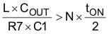
When a ceramic output capacitor is used, the stability criteria in Equation 7 cannot be satisfied. The ripple injection approach as shown in Figure 8-2 is implemented to increase the ripple on the VFB pin and make the system stable. In addition to the selections made using steps 1 through step 6 in Section 8.2.1.2.2, the ripple injection components must be selected. The C2 value can be fixed at 1 nF. The value of C1 can be selected between 10 nF to 200 nF.
where
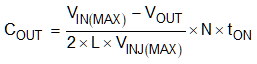
- N is the coefficient to account for L and COUT variation
N is also used to provide enough margin for stability. It is recommended N=2 for VOUT ≤ 1.8 V and N=4 for VOUT ≥ 3.3 V or when L ≤ 250 nH. The higher VOUT needs a higher N value because the effective output capacitance is reduced significantly with higher DC bias. For example, a 6.3-V, 22-µF ceramic capacitor may have only 8 µF of effective capacitance when biased at 5 V.
Because the VFB pin voltage is regulated at the valley, the increased ripple on the VFB pin causes the increase of the VFB DC value. The AC ripple coupled to the VFB pin has two components, one coupled from SW node and the other coupled from the VOUT pin and they can be calculated using Equation 12 and Equation 13 when neglecting the output voltage ripple caused by equivalent series inductance (ESL).
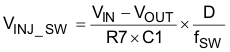
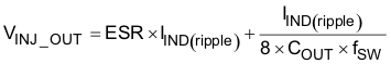
It is recommended that VINJ_SW to be less than 50 mV and VINJ_TOTAL to be less than 60 mV. If the calculated VINJ_SW is higher than 50 mV, then other parameters need to be adjusted to reduce it. For example, COUT can be increased to satisfy Equation 11 with a higher R7 value, thereby reducing VINJ_SW. Use Equation 14 to calculate COUT capacitance needed. For a more holistic calculation, please reference the TPS53355 calculator on ti.com
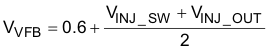
The DC voltage at the VFB pin can be calculated by Equation 15:
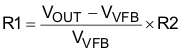
And the resistor divider value can be determined by Equation 16: