JAJSOW4A September 2009 – January 2024 TPS5410-Q1
PRODUCTION DATA
- 1
- 1特長
- 2アプリケーション
- 3概要
- 4静電気放電に関する注意事項
- 5Ordering Information
- 6Pin Assignments
- 7Specifications
-
8Application Information
- 8.1 Functional Block Diagram
- 8.2
Detailed Description
- 8.2.1 Oscillator Frequency
- 8.2.2 Voltage Reference
- 8.2.3 Enable (ENA) and Internal Slow Start
- 8.2.4 Undervoltage Lockout (UVLO)
- 8.2.5 Boost Capacitor (BOOT)
- 8.2.6 Output Feedback (VSENSE)
- 8.2.7 Internal Compensation
- 8.2.8 Voltage Feed Forward
- 8.2.9 Pulse-Width-Modulation (PWM) Control
- 8.2.10 Overcurrent Liming
- 8.2.11 Overvoltage Protection
- 8.2.12 Thermal Shutdown
- 8.2.13 PCB Layout
- 8.2.14 Application Circuits
- 8.2.15 Design Procedure
- 8.2.16 Output Filter Capacitor Selection
- 8.2.17 External Compensation Network
- 8.3 Advanced Information
- 8.4 Performance Graphs
- 8.5 Performance Graphs
- 9Revision History
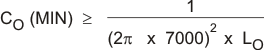
8.2.16 Output Filter Capacitor Selection
When using ceramic output filer capacitors, the recommended LC resonant frequency should be no more than 7 kHz. Since the output inductor is already selected at 68 μH, this limits the minimum output capacitor value to:
The minimum capacitor value is calculated to be 7.6 μF. For this circuit a larger value of capacitor will yield better transient response. Two output capacitors are used for C3 and C4 with a value of 47 uF each. It is important to note that the actual capacitance of ceramic capacitors decreases with applied voltage. In this case the effective value used for the calculations is approximately 70 % of the rated value or 70 μF.