JAJS448D March 2010 – October 2018 TPS54260
PRODUCTION DATA.
- 1 特長
- 2 アプリケーション
- 3 概要
- 4 改訂履歴
- 5 概要(続き)
- 6 Pin Configuration and Functions
- 7 Specifications
-
8 Detailed Description
- 8.1 Overview
- 8.2 Functional Block Diagram
- 8.3
Feature Description
- 8.3.1 Fixed Frequency PWM Control
- 8.3.2 Slope Compensation Output Current
- 8.3.3 Pulse-Skip Eco-Mode
- 8.3.4 Low-Dropout Operation and Bootstrap Voltage (BOOT)
- 8.3.5 Error Amplifier
- 8.3.6 Voltage Reference
- 8.3.7 Adjusting the Output Voltage
- 8.3.8 Enable and Adjusting Undervoltage Lockout
- 8.3.9 Slow-Start / Tracking Pin (SS/TR)
- 8.3.10 Overload Recovery Circuit
- 8.3.11 Sequencing
- 8.3.12 Constant Switching Frequency and Timing Resistor (RT/CLK Pin)
- 8.3.13 Overcurrent Protection and Frequency Shift
- 8.3.14 Selecting the Switching Frequency
- 8.3.15 How to Interface to RT/CLK Pin
- 8.3.16 Powergood (PWRGD Pin)
- 8.3.17 Overvoltage Transient Protection
- 8.3.18 Thermal Shutdown
- 8.3.19 Small Signal Model for Loop Response
- 8.3.20 Simple Small Signal Model for Peak Current Mode Control
- 8.3.21 Small Signal Model for Frequency Compensation
- 8.4 Device Functional Modes
-
9 Application and Implementation
- 9.1 Application Information
- 9.2
Typical Applications
- 9.2.1
3.3-V Output Application
- 9.2.1.1 Design Requirements
- 9.2.1.2
Detailed Design Procedure
- 9.2.1.2.1 Custom Design With WEBENCH® Tools
- 9.2.1.2.2 Selecting the Switching Frequency
- 9.2.1.2.3 Output Inductor Selection (LO)
- 9.2.1.2.4 Output Capacitor
- 9.2.1.2.5 Catch Diode
- 9.2.1.2.6 Input Capacitor
- 9.2.1.2.7 Slow-Start Capacitor
- 9.2.1.2.8 Bootstrap Capacitor Selection
- 9.2.1.2.9 Undervoltage Lock Out Set Point
- 9.2.1.2.10 Output Voltage and Feedback Resistors Selection
- 9.2.1.2.11 Compensation
- 9.2.1.2.12 Discontinuous Mode and Eco-Mode Boundary
- 9.2.1.2.13 Power Dissipation Estimate
- 9.2.1.3 Application Curves
- 9.2.2 Inverting Power Supply
- 9.2.3 Split-Rail Power Supply
- 9.2.4 12-V to 3.8-V GSM Power Supply
- 9.2.5 24-V to 4.2-V GSM Power Supply
- 9.2.1
3.3-V Output Application
- 10Power Supply Recommendations
- 11Layout
- 12デバイスおよびドキュメントのサポート
- 13メカニカル、パッケージ、および注文情報
パッケージ・オプション
メカニカル・データ(パッケージ|ピン)
サーマルパッド・メカニカル・データ
発注情報
8.3.14 Selecting the Switching Frequency
The switching frequency that is selected should be the lower value of the two equations, Equation 12 and Equation 13. Equation 12 is the maximum switching frequency limitation set by the minimum controllable on time. Setting the switching frequency above this value will cause the regulator to skip switching pulses.
Equation 13 is the maximum switching frequency limit set by the frequency shift protection. To have adequate output short circuit protection at high input voltages, the switching frequency should be set to be less than the fsw(maxshift) frequency. In Equation 13, to calculate the maximum switching frequency one must take into account that the output voltage decreases from the nominal voltage to 0 V, the fdiv integer increases from 1 to 8 corresponding to the frequency shift.
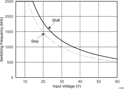
In Figure 41, the solid line illustrates a typical safe operating area regarding frequency shift and assumes the output voltage is 0 V, and the resistance of the inductor is 0.130 Ω, FET on resistance of 0.2 Ω and the diode voltage drop is 0.5 V. The dashed line is the maximum switching frequency to avoid pulse skipping. Enter these equations in a spreadsheet or other software or use the SwitcherPro design software to determine the switching frequency.


where
- IL = inductor current
- Rdc = inductor resistance
- VIN = maximum input voltage
- VOUT = output voltage
- VOUTSC =output voltage during short
- Vd = diode voltage drop
- RDS(on) = switch on resistance
- tON = controllable on time
- ƒDIV = frequency divide equals (1, 2, 4, or 8)
 Figure 41. Maximum Switching Frequency vs Input Voltage