JAJSD91A June 2017 – April 2021 TPS54308
PRODUCTION DATA
- 1 特長
- 2 アプリケーション
- 3 概要
- 4 Revision History
- 5 Pin Configuration and Functions
- 6 Specifications
-
7 Detailed Description
- 7.1 Overview
- 7.2 Functional Block Diagram
- 7.3
Feature Description
- 7.3.1 Fixed-Frequency PWM Control
- 7.3.2 Force Continuous Conduction Mode (FCCM)
- 7.3.3 Error Amplifier
- 7.3.4 Slope Compensation and Output Current
- 7.3.5 Enable and Adjusting Undervoltage Lockout
- 7.3.6 Safe Start-Up into Pre-Biased Outputs
- 7.3.7 Voltage Reference
- 7.3.8 Adjusting Output Voltage
- 7.3.9 Internal Soft Start
- 7.3.10 Bootstrap Voltage (BOOT)
- 7.3.11 Overcurrent Protection
- 7.3.12 Output Overvoltage Protection (OVP)
- 7.3.13 Thermal Shutdown
- 7.4 Device Functional Modes
-
8 Application and Implementation
- 8.1 Application Information
- 8.2
Typical Application
- 8.2.1 TPS54308 8-V to 28-V Input, 5-V Output Converter
- 8.2.2 Design Requirements
- 8.2.3 Detailed Design Procedure
- 8.2.4 Application Curves
- 9 Power Supply Recommendations
- 10Layout
- 11Device and Documentation Support
- 12Mechanical, Packaging, and Orderable Information
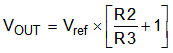
7.3.8 Adjusting Output Voltage
The output voltage is set with a resistor divider from the output node to the FB pin. It is recommended to use divider resistors with 1% tolerance or better. Start with 100 kΩ for the upper resistor divider. Use Equation 3 to calculate the output voltage. To improve efficiency at ligh,t loads, consider using larger value resistors. If the values are too high the regulator is more susceptible to noise and voltage errors from the FB input current are noticeable.
Equation 3.