JAJSJI7A April   2017  – September 2020 TPS561201 , TPS561208

PRODUCTION DATA  

  1. 特長
  2. アプリケーション
  3. 概要
  4. Revision History
  5. Pin Configuration and Functions
    1.     Pin Functions
  6. Specifications
    1. 6.1 Absolute Maximum Ratings
    2. 6.2 ESD Ratings
    3. 6.3 Recommended Operating Conditions
    4. 6.4 Thermal Information
    5. 6.5 Electrical Characteristics
    6. 6.6 Typical Characteristics
  7. Detailed Description
    1. 7.1 Overview
    2. 7.2 Functional Block Diagram
    3. 7.3 Feature Description
      1. 7.3.1 Adaptive On-Time Control and PWM Operation
      2. 7.3.2 Pulse Skip Control (TPS561201)
      3. 7.3.3 Soft Start and Pre-Biased Soft Start
      4. 7.3.4 Current Protection
      5. 7.3.5 Undervoltage Lockout (UVLO) Protection
      6. 7.3.6 Thermal Shutdown
    4. 7.4 Device Functional Modes
      1. 7.4.1 Normal Operation
      2. 7.4.2 Eco-mode Operation
      3. 7.4.3 Standby Operation
  8. Application and Implementation
    1. 8.1 Application Information
    2. 8.2 Typical Application
      1. 8.2.1 Design Requirements
      2. 8.2.2 Detailed Design Procedure
        1. 8.2.2.1 Custom Design With WEBENCH® Tools
        2. 8.2.2.2 Output Voltage Resistors Selection
        3. 8.2.2.3 Output Filter Selection
        4. 8.2.2.4 Input Capacitor Selection
        5. 8.2.2.5 Bootstrap Capacitor Selection
      3. 8.2.3 Application Curves
  9. Power Supply Recommendations
  10. 10Layout
    1. 10.1 Layout Guidelines
    2. 10.2 Layout Example
  11. 11Device and Documentation Support
    1. 11.1 Device Support
      1. 11.1.1 Development Support
        1. 11.1.1.1 Custom Design With WEBENCH® Tools
    2. 11.2 Receiving Notification of Documentation Updates
    3. 11.3 Support Resources
    4. 11.4 Trademarks
    5. 11.5 Electrostatic Discharge Caution
    6. 11.6 Glossary
  12. 12Mechanical, Packaging, and Orderable Information

パッケージ・オプション

メカニカル・データ(パッケージ|ピン)
サーマルパッド・メカニカル・データ
発注情報

Typical Application

The application schematic in Figure 8-1 was developed to meet the previous requirements. This circuit is available as the evaluation module (EVM). The sections provide the design procedure.

Figure 8-1 shows the TPS561201 and TPS561208 4.5-V to 17-V Input, 1.05-V output converter schematics.
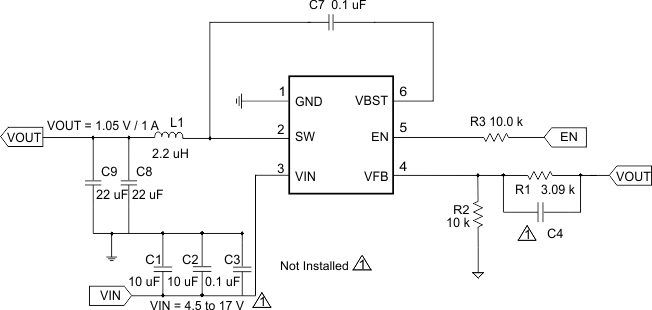
GUID-AC7E157D-C562-4BD1-B856-5E084E745DA8-low.gifFigure 8-1 TPS561201 and TPS561208 1.05-V/1-A Reference Design