JAJSC03E january   2014  – may 2023 TPS562200 , TPS563200

PRODUCTION DATA  

  1.   1
  2. 特長
  3. アプリケーション
  4. 概要
  5. Revision History
  6. Pin Configuration and Functions
  7. Specifications
    1. 6.1 Absolute Maximum Ratings #GUID-10807E29-2FD4-4A3F-94B2-FDEBD147A133/SLVSC819633
    2. 6.2 ESD Ratings
    3. 6.3 Recommended Operating Conditions
    4. 6.4 Thermal Information
    5. 6.5 Electrical Characteristics
    6. 6.6 Timing Requirements
    7. 6.7 Typical Characteristics TPS562200
    8. 6.8 Typical Characteristics TPS563200
  8. Detailed Description
    1. 7.1 Overview
    2. 7.2 Functional Block Diagram
    3. 7.3 Feature Description
      1. 7.3.1 The Adaptive On-Time Control And PWM Operation
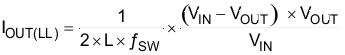
      2. 7.3.2 Advanced Eco-mode Control
      3. 7.3.3 Soft Start And Pre-Biased Soft Start
      4. 7.3.4 Current Protection
      5. 7.3.5 Over Voltage Protection
      6. 7.3.6 UVLO Protection
      7. 7.3.7 Thermal Shutdown
    4. 7.4 Device Functional Modes
      1. 7.4.1 Normal Operation
      2. 7.4.2 Eco-mode Operation
      3. 7.4.3 Standby Operation
  9. Application and Implementation
    1. 8.1 Application Information
    2. 8.2 Typical Applications
      1. 8.2.1 Tps562200 4.5-V To 17-V Input, 1.05-V Output Converter
        1. 8.2.1.1 Design Requirements
        2. 8.2.1.2 Detailed Design Procedures
          1. 8.2.1.2.1 Custom Design with WEBENCH® Tools
          2. 8.2.1.2.2 Output Voltage Resistors Selection
          3. 8.2.1.2.3 Output Filter Selection
          4. 8.2.1.2.4 Input Capacitor Selection
          5. 8.2.1.2.5 Bootstrap Capacitor Selection
        3. 8.2.1.3 Application Curves
      2. 8.2.2 Tps563200 4.5-V To 17-V Input, 1.05-V Output Converter
        1. 8.2.2.1 Design Requirements
        2. 8.2.2.2 Detailed Design Procedures
          1. 8.2.2.2.1 Output Filter Selection
        3. 8.2.2.3 Application Curves
    3. 8.3 Power Supply Recommendations
    4. 8.4 Layout
      1. 8.4.1 Layout Guidelines
      2. 8.4.2 Layout Example
  10. Device and Documentation Support
    1. 9.1 Device Support
      1. 9.1.1 Development Support
        1. 9.1.1.1 Custom Design with WEBENCH® Tools
    2. 9.2 ドキュメントの更新通知を受け取る方法
    3. 9.3 サポート・リソース
    4. 9.4 Trademarks
    5. 9.5 静電気放電に関する注意事項
    6. 9.6 用語集
  11. 10Mechanical, Packaging, And Orderable Information

パッケージ・オプション

メカニカル・データ(パッケージ|ピン)
サーマルパッド・メカニカル・データ
発注情報

Advanced Eco-mode Control

The TPS562200 and TPS563200 are designed with Advanced Eco-mode to maintain high light load efficiency. As the output current decreases from heavy load condition, the inductor current is also reduced and eventually comes to point that its rippled valley touches zero level, which is the boundary between continuous conduction and discontinuous conduction modes. The rectifying MOSFET is turned off when the zero inductor current is detected. As the load current further decreases, the converter runs into discontinuous conduction mode. The on-time is kept almost the same as it was in the continuous conduction mode so that it takes longer time to discharge the output capacitor with smaller load current to the level of the reference voltage. This makes the switching frequency lower, proportional to the load current, and keeps the light load efficiency high. The transition point to the light load operation IOUT(LL) current can be calculated in Equation 1.

Equation 1. GUID-724F674F-8FE1-476F-9766-A2045D1F7A06-low.gif