JAJSCP3 November   2016 TPS562210A , TPS563210A

PRODUCTION DATA.  

  1. 特長
  2. アプリケーション
  3. 概要
  4. 改訂履歴
  5. Pin Configuration and Functions
  6. Specifications
    1. 6.1 Absolute Maximum Ratings
    2. 6.2 ESD Ratings
    3. 6.3 Recommended Operating Conditions
    4. 6.4 Thermal Information
    5. 6.5 Electrical Characteristics
    6. 6.6 Timing Requirements
    7. 6.7 Typical Characteristics
      1. 6.7.1 TPS562210A Characteristics
      2. 6.7.2 TPS563210A Characteristics
  7. Detailed Description
    1. 7.1 Overview
    2. 7.2 Functional Block Diagram
    3. 7.3 Feature Description
      1. 7.3.1 The Adaptive On-Time Control and PWM Operation
      2. 7.3.2 Soft Start and Pre-Biased Soft Start
      3. 7.3.3 Power Good
      4. 7.3.4 Current Protection
      5. 7.3.5 Over Voltage Protection
      6. 7.3.6 UVLO Protection
      7. 7.3.7 Thermal Shutdown
    4. 7.4 Device Functional Modes
      1. 7.4.1 Advanced Eco-Mode™ Control
  8. Application and Implementation
    1. 8.1 Application Information
    2. 8.2 Typical Application
      1. 8.2.1 Typical Application, TPS562210A
        1. 8.2.1.1 Design Requirements
        2. 8.2.1.2 Detailed Design Procedure
          1. 8.2.1.2.1 Output Voltage Resistors Selection
          2. 8.2.1.2.2 Output Filter Selection
          3. 8.2.1.2.3 Input Capacitor Selection
          4. 8.2.1.2.4 Bootstrap capacitor Selection
        3. 8.2.1.3 Application Curves
      2. 8.2.2 Typical Application, TPS563210A
        1. 8.2.2.1 Design Requirements
        2. 8.2.2.2 Detailed Design Procedures
          1. 8.2.2.2.1 Output Filter Selection
        3. 8.2.2.3 Application Curves
  9. Power Supply Recommendations
  10. 10Layout
    1. 10.1 Layout Guidelines
    2. 10.2 Layout Example
  11. 11デバイスおよびドキュメントのサポート
    1. 11.1 デバイス・サポート
    2. 11.2 関連リンク
    3. 11.3 ドキュメントの更新通知を受け取る方法
    4. 11.4 コミュニティ・リソース
    5. 11.5 商標
    6. 11.6 静電気放電に関する注意事項
    7. 11.7 用語集
  12. 12メカニカル、パッケージ、および注文情報

パッケージ・オプション

メカニカル・データ(パッケージ|ピン)
サーマルパッド・メカニカル・データ
発注情報

Pin Configuration and Functions

DDF Package
8 Pin
Top View
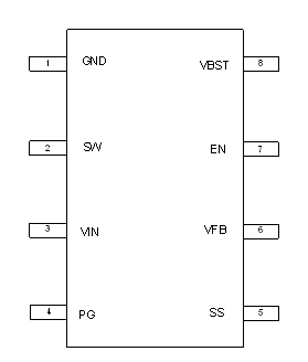
TPS562210A TPS563210A po_slvscm6.gif

Pin Functions

PIN DESCRIPTION
NAME NO.
GND 1 Ground pin Source terminal of low-side power NFET as well as the ground terminal for controller circuit. Connect sensitive VFB to this GND at a single point.
SW 2 Switch node connection between high-side NFET and low-side NFET.
VIN 3 Input voltage supply pin. The drain terminal of high-side power NFET.
PG 4 Power good open drain output
SS 5 Soft-start control. An external capacitor should be connected to GND.
VFB 6 Converter feedback input. Connect to output voltage with feedback resistor divider.
EN 7 Enable input control. Active high and must be pulled up to enable the device.
VBST 8 Supply input for the high-side NFET gate drive circuit. Connect 0.1 µF capacitor between VBST and SW pins.