JAJSGE5C March 2019 – August 2019 TPS568230
PRODUCTION DATA.
- 1 特長
- 2 アプリケーション
- 3 概要
- 4 改訂履歴
- 5 概要(続き)
- 6 Pin Configuration and Functions
- 7 Specifications
- 8 Detailed Description
- 9 Application and Implementation
- 10Power Supply Recommendations
- 11Layout
- 12デバイスおよびドキュメントのサポート
- 13メカニカル、パッケージ、および注文情報
8.4.5 Mode Selection
The device reads the voltage on the MODE pin during start-up and latches onto one of the MODE options listed below in Table 1 . The voltage on the MODE pin can be set by connecting this pin to the center tap of a resistor divider connected between VCC and AGND. A guideline for the top resistor (RM_H) and the bottom resistor (RM_L) is shown in Table 1, and 1% resistors are recommended. It is important that the voltage for the MODE pin is derived from the VCC rail only since internally this voltage is referenced to detect the MODE option. The MODE pin setting can be reset only by a VIN power cycling or EN toggle.
Table 1. MODE Pin Resistor Settings
| RM_H(kΩ) | RM_L (kΩ) | LIGHT LOAD OPERATION | SWITCHING FREQUENCY (kHz) |
|---|---|---|---|
| 330 | 5.1 | Eco-mode | 600 |
| 330 | 15 | Eco-mode | 800 |
| 330 | 27 | Eco-mode | 1000 |
| 300 | 43 | OOA mode | 600 |
| 150 | 33 | OOA mode | 800 |
| 160 | 51 | OOA mode | 1000 |
| 110 | 51 | FCCM | 600 |
| 75 | 51 | FCCM | 800 |
| 51 | 51 | FCCM | 1000 |
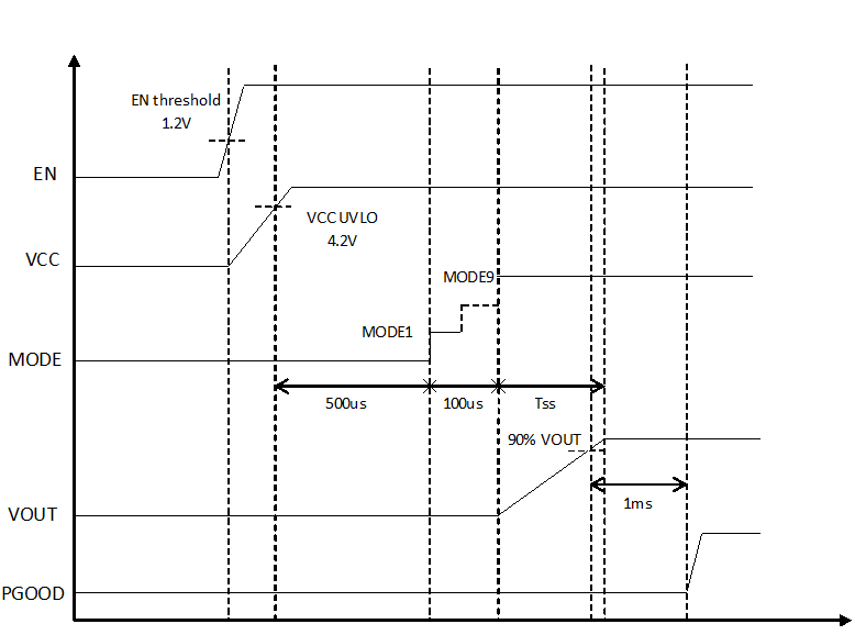
Figure 29 below shows the typical start-up sequence of the device once the enable signal crosses the EN turn on threshold. After the voltage on VCC crosses the rising UVLO threshold it takes about 500us to read the first mode setting and approximately 100us from there to finish the last mode setting. The output voltage starts ramping after the mode reading is done.
 Figure 29. Power-Up Sequence