JAJSGY7B September 2017 – February 2019 TPS61085A-Q1
PRODUCTION DATA.
6.6 Typical Characteristics
The typical characteristics are measured with the 3.3-µH inductor for high-frequency (part number-7447789003) or 6.8-µH inductor for low frequency (part number-B82464G4) and the rectifier diode with part number SL22.Table 1. Table of Graphs
| FIGURE | |||
|---|---|---|---|
| IOUT(max) | Maximum load current | vs Input voltage at high frequency (1.2 MHz) | Figure 1 |
| vs Input voltage at low frequency (650 kHz) | Figure 2 | ||
| η | Efficiency | vs Load current, VS = 12 V, VIN = 3.3 V | Figure 3 |
| vs Load current, VS = 9 V, VIN = 3.3 V | Figure 4 | ||
| Supply current | vs Supply voltage | Figure 5 | |
| Frequency | vs Load current | Figure 6 | |
| vs Supply voltage | Figure 7 | ||
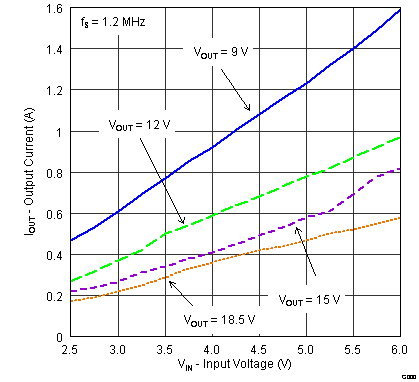 Figure 1. Maximum Load Current vs Input Voltage
 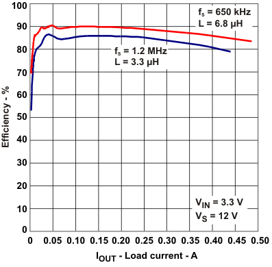 Figure 3. Efficiency vs Load Current, VS = 12 V, VIN = 3.3 V
 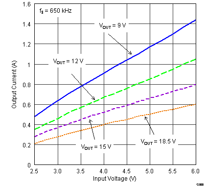 Figure 2. Maximum Load Current vs Input Voltage
 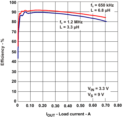 Figure 4. Efficiency vs Load Current, VS = 9 V, VIN = 3.3 V
 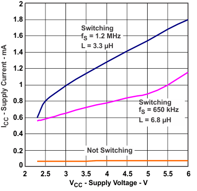 Figure 5. Supply Current vs Supply Voltage
 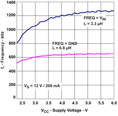 Figure 7. Frequency vs Supply Voltage
 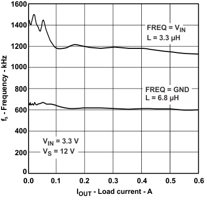 Figure 6. Frequency vs Load Current