JAJSGB2D May   2015  – August 2021 TPS61088

PRODUCTION DATA  

  1. 特長
  2. アプリケーション
  3. 概要
  4. Revision History
  5. Pin Configuration and Functions
  6. Specifications
    1. 6.1 Absolute Maximum Ratings
    2. 6.2 ESD Ratings
    3. 6.3 Recommended Operating Conditions
    4. 6.4 Thermal Information
    5. 6.5 Electrical Characteristics
    6. 6.6 Typical Characteristics
  7. Detailed Description
    1. 7.1 Overview
    2. 7.2 Functional Block Diagram
    3. 7.3 Feature Description
      1. 7.3.1 Enable and Start-up
      2. 7.3.2 Undervoltage Lockout (UVLO)
      3. 7.3.3 Adjustable Switching Frequency
      4. 7.3.4 Adjustable Peak Current Limit
      5. 7.3.5 Overvoltage Protection
      6. 7.3.6 Thermal Shutdown
    4. 7.4 Device Functional Modes
      1. 7.4.1 Operation
        1. 7.4.1.1 PWM Mode
        2. 7.4.1.2 PFM Mode
  8. Application and Implementation
    1. 8.1 Application Information
    2. 8.2 Typical Application
      1. 8.2.1 Design Requirements
      2. 8.2.2 Detailed Design Procedure
        1. 8.2.2.1 Custom Design with WEBENCH Tools
        2. 8.2.2.2 Setting Switching Frequency
        3. 8.2.2.3 Setting Peak Current Limit
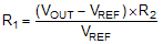
        4. 8.2.2.4 Setting Output Voltage
        5. 8.2.2.5 Inductor Selection
        6. 8.2.2.6 Input Capacitor Selection
        7. 8.2.2.7 Output Capacitor Selection
        8. 8.2.2.8 Loop Stability
      3. 8.2.3 Application Curves
  9. Power Supply Recommendations
  10. 10Layout
    1. 10.1 Layout Guidelines
    2. 10.2 Layout Example
    3. 10.3 Thermal Considerations
  11. 11Device and Documentation Support
    1. 11.1 Device Support
      1. 11.1.1 Third-Party Products Disclaimer
      2. 11.1.2 Development Support
        1. 11.1.2.1 Custom Design with WEBENCH Tools
    2. 11.2 Receiving Notification of Documentation Updates
    3. 11.3 サポート・リソース
    4. 11.4 Trademarks
    5. 11.5 Electrostatic Discharge Caution
    6. 11.6 Glossary
  12. 12Mechanical, Packaging, and Orderable Information

パッケージ・オプション

メカニカル・データ(パッケージ|ピン)
サーマルパッド・メカニカル・データ
発注情報

Setting Output Voltage

The output voltage is set by an external resistor divider (R1, R2 in Figure 8-1). Typically, a minimum current of 20 μA flowing through the feedback divider gives good accuracy and noise covering. A standard 56-kΩ resistor is typically selected for low-side resistor R2.

The value of R1 is then calculated as:

Equation 7. GUID-02C08AF2-CBDE-4735-921E-58A9B1211B28-low.gif