JAJSJ58B january 2015 – august 2023 TPS62065-Q1 , TPS62067-Q1
PRODUCTION DATA
- 1
- 1 特長
- 2 アプリケーション
- 3 概要
- 4 Revision History
- 5 Device Comparison Table
- 6 Pin Configuration and Functions
- 7 Specifications
- 8 Parameter Measurement Information
-
9 Detailed Description
- 9.1 Overview
- 9.2 Functional Block Diagram
- 9.3
Feature Description
- 9.3.1 Mode Selection (TPS62065-Q1) and Forced PWM Mode (TPS62067A-Q1)
- 9.3.2 Power Good (PG, TPS62067x-Q1)
- 9.3.3 Enable
- 9.3.4 Shutdown and Output Discharge
- 9.3.5 Soft Start
- 9.3.6 Undervoltage Lockout (UVLO)
- 9.3.7 Internal Current Limit and Foldback Current Limit For Short-Circuit Protection
- 9.3.8 Clock Dithering
- 9.3.9 Thermal Shutdown
- 9.4 Device Functional Modes
- 10Application and Implementation
- 11Device and Documentation Support
- 12Mechanical, Packaging, and Orderable Information
パッケージ・オプション
メカニカル・データ(パッケージ|ピン)
- DSG|8
サーマルパッド・メカニカル・データ
- DSG|8
発注情報
10.2.2.2 Output Filter Design (Inductor And Output Capacitor)
The internal compensation network of the devices is optimized for a LC output filter with a corner frequency of:
Equation 5. 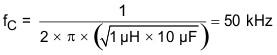
The part operates with nominal inductors of 1 µH to 1.2 µH and with 10-µF to 22-µF small X5R and X7R ceramic capacitors. Refer to the lists of inductors and capacitors. The part is optimized for a 1-µH inductor and 10-µF output capacitor.