JAJSHO1C May 2014 – July 2019 TPS62150A-Q1 , TPS62152A-Q1 , TPS62153A-Q1
PRODUCTION DATA.
- 1 特長
- 2 アプリケーション
- 3 概要
- 4 改訂履歴
- 5 Device Comparison Table
- 6 Pin Configuration and Functions
- 7 Specifications
- 8 Parameter Measurement Information
-
9 Detailed Description
- 9.1 Overview
- 9.2 Functional Block Diagram
- 9.3
Feature Description
- 9.3.1 Pulse Width Modulation (PWM) Operation
- 9.3.2 Power Save Mode Operation
- 9.3.3 100% Duty-Cycle Operation
- 9.3.4 Enable / Shutdown (EN)
- 9.3.5 Soft Start / Tracking (SS/TR)
- 9.3.6 Current Limit And Short Circuit Protection
- 9.3.7 Power Good (PG)
- 9.3.8 Pin-Selectable Output Voltage (DEF)
- 9.3.9 Frequency Selection (FSW)
- 9.3.10 Under Voltage Lockout (UVLO)
- 9.3.11 Thermal Shutdown
- 9.4 Device Functional Modes
-
10Application and Implementation
- 10.1 Application Information
- 10.2
Typical Application
- 10.2.1
TPS62150A-Q1 Point-Of-Load Step Down Converter
- 10.2.1.1 Design Requirements
- 10.2.1.2
Detailed Design Procedure
- 10.2.1.2.1 Custom Design With WEBENCH® Tools
- 10.2.1.2.2 Programming The Output Voltage
- 10.2.1.2.3 External Component Selection
- 10.2.1.2.4 Inductor Selection
- 10.2.1.2.5 Output Capacitor
- 10.2.1.2.6 Input Capacitor
- 10.2.1.2.7 Soft Start Capacitor
- 10.2.1.2.8 Tracking Function
- 10.2.1.2.9 Output Filter And Loop Stability
- 10.2.1.3 Application Curves
- 10.2.2 System Examples
- 10.2.1
TPS62150A-Q1 Point-Of-Load Step Down Converter
- 11Power Supply Recommendations
- 12Layout
- 13デバイスおよびドキュメントのサポート
- 14メカニカル、パッケージ、および注文情報
パッケージ・オプション
デバイスごとのパッケージ図は、PDF版データシートをご参照ください。
メカニカル・データ(パッケージ|ピン)
- RGT|16
サーマルパッド・メカニカル・データ
発注情報
10.2.1.2.4 Inductor Selection
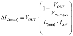
The inductor selection is affected by several effects like inductor ripple current, output ripple voltage, PWM-to-PSM transition point and efficiency. In addition, the inductor selected has to be rated for appropriate saturation current and DC resistance (DCR). Equation 7 and Equation 8 calculate the maximum inductor current under static load conditions.
spacing

spacing

where
IL(max) is the maximum inductor current,
ΔIL is the Peak to Peak Inductor Ripple Current,
L(min) is the minimum effective inductor value and
fSW is the actual PWM Switching Frequency.
spacing
Calculating the maximum inductor current using the actual operating conditions gives the minimum saturation current of the inductor needed. A margin of about 20% is recommended to add. A larger inductor value is also useful to get lower ripple current, but increases the transient response time and solution size as well. The following inductors have been used with the TPS6215xA-Q1 and are recommended for use:
Table 4. List of Inductors(1)
| Type | Inductance [µH] | Current [A](2) | Dimensions [LxBxH] mm | MANUFACTURER |
|---|---|---|---|---|
| XFL4020-102ME_ | 1.0 µH, ±20% | 4.7 | 4 x 4 x 2.1 | Coilcraft |
| XFL4020-152ME_ | 1.5 µH, ±20% | 4.2 | 4 x 4 x 2.1 | Coilcraft |
| XFL4020-222ME_ | 2.2 µH, ±20% | 3.8 | 4 x 4 x 2.1 | Coilcraft |
| IHLP1212BZ-11 | 1.0 µH, ±20% | 4.5 | 3 x 3.6 x 2 | Vishay |
| IHLP1212BZ-11 | 2.2 µH, ±20% | 3.0 | 3 x 3.6 x 2 | Vishay |
| SRP4020-3R3M | 3.3µH, ±20% | 3.3 | 4.8 x 4 x 2 | Bourns |
| VLC5045T-3R3N | 3.3µH, ±30% | 4.0 | 5 x 5 x 4.5 | TDK |
spacing
The inductor value also determines the load current at which Power Save Mode is entered:

Using Equation 8, this current level can be adjusted by changing the inductor value.