JAJSLH2 March 2021 TPS62810M , TPS62811M , TPS62812M , TPS62813M
PRODUCTION DATA
- 1 特長
- 2 アプリケーション
- 3 概要
- 4 Revision History
- 5 Device Comparison Table
- 6 Pin Configuration and Functions
- 7 Specifications
- 8 Parameter Measurement Information
- 9 Detailed Description
- 10Application and Implementation
- 11Power Supply Recommendations
- 12Layout
- 13Device and Documentation Support
- 14Mechanical, Packaging, and Orderable Information
パッケージ・オプション
メカニカル・データ(パッケージ|ピン)
- RWY|9
サーマルパッド・メカニカル・データ
- RWY|9
発注情報
10.1.2 Inductor Selection
The TPS6281xM device is designed for a nominal 0.47-µH inductor with a typical switching frequency of 2.25 MHz. Larger values can be used to achieve a lower inductor current ripple, but they can have a negative impact on efficiency and transient response. Smaller values than 0.47 µH cause a larger inductor current ripple, which causes larger negative inductor current in forced PWM mode at low or no output current. For a higher or lower nominal switching frequency, the inductance must be changed accordingly.
The inductor selection is affected by several effects like the following:
- Inductor ripple current
- Output ripple voltage
- PWM-to-PFM transition point
- Efficiency
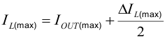
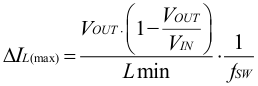
where
- IL(max) is the maximum inductor current
- ΔIL(max) is the peak-to-peak inductor ripple current
- Lmin is the minimum inductance at the operating point
| TYPE | INDUCTANCE [µH] | CURRENT [A] (1) | FOR DEVICE | NOMINAL SWITCHING FREQUENCY | DIMENSIONS [LxBxH] mm | MANUFACTURER(2) |
OPERATION AT –55°C |
|---|---|---|---|---|---|---|---|
| ML433PYA601MLZ | 0.6 µH, ±20% | 10.4 | TPS62810M, TPS62813M, TPS62812M | 2.25 MHz | 4 × 4 × 2.1 | Coilcraft |
yes |
| ML433PYA401MLZ | 0.4 µH, ±20% | 12.5 | TPS62810M, TPS62813M, TPS62812M | 2.25 MHz | 4 × 4 × 2.1 | Coilcraft |
yes |
| XFL4015-471ME | 0.47 µH, ±20% | 3.5 | TPS62813M, TPS62812M | 2.25 MHz | 4 × 4 × 1.6 | Coilcraft |
no |
| XEL4020-561ME | 0.56 µH, ±20% | 9.9 | TPS62810M, TPS62813M, TPS62812M | 2.25 MHz | 4 × 4 × 2.1 | Coilcraft |
no |
| XEL4030-471ME | 0.47 µH, ±20% | 12.3 | TPS62810M, TPS62813M, TPS62812M | 2.25 MHz | 4 × 4 × 3.1 | Coilcraft |
no |
| XEL3515-561ME | 0.56 µH, ±20% | 4.5 | TPS62813M, TPS62812M | 2.25 MHz | 3.5 × 3.2 × 1.5 | Coilcraft |
no |
| XFL3012-331MEB | 0.33 µH, ±20% | 2.6 | TPS62811M, TPS62812M | ≥ 3.5 MHz | 3 × 3 × 1.3 | Coilcraft |
no |
| XPL2010-681ML | 0.68 µH, ±20% | 1.5 | TPS62811M | 2.25 MHz | 2 × 1.9 × 1 | Coilcraft |
no |
| DFE252012PD-R47M | 0.47 µH, ±20% | see data sheet | TPS62811M, TPS62813M, TPS62812M | 2.25 MHz | 2.5 × 2 × 1.2 | Murata |
no |
Calculating the maximum inductor current using the actual operating conditions gives the minimum saturation current of the inductor needed. A margin of about 20% is recommended to add. A larger inductor value is also useful to get lower ripple current, but increases the transient response time and size as well.