JAJSJ61J May   2020  – November 2023 TPS628501-Q1 , TPS628502-Q1 , TPS628503-Q1

PRODUCTION DATA  

  1.   1
  2. 特長
  3. アプリケーション
  4. 概要
  5. Device Comparison Table
  6. Pin Configuration and Functions
  7. Specifications
    1. 6.1 Absolute Maximum Ratings
    2. 6.2 ESD Ratings
    3. 6.3 Recommended Operating Conditions
    4. 6.4 Thermal Information
    5. 6.5 Electrical Characteristics
    6. 6.6 Typical Characteristics
  8. Parameter Measurement Information
    1. 7.1 Schematic
  9. Detailed Description
    1. 8.1 Overview
    2. 8.2 Functional Block Diagram
    3. 8.3 Feature Description
      1. 8.3.1 Precise Enable (EN)
      2. 8.3.2 COMP/FSET
      3. 8.3.3 MODE / SYNC
      4. 8.3.4 Spread Spectrum Clocking (SSC)
      5. 8.3.5 Undervoltage Lockout (UVLO)
      6. 8.3.6 Power-Good Output (PG)
      7. 8.3.7 Thermal Shutdown
    4. 8.4 Device Functional Modes
      1. 8.4.1 Pulse Width Modulation (PWM) Operation
      2. 8.4.2 Power Save Mode Operation (PWM/PFM)
      3. 8.4.3 100% Duty-Cycle Operation
      4. 8.4.4 Current Limit and Short Circuit Protection
      5. 8.4.5 Foldback Current Limit and Short-Circuit Protection
      6. 8.4.6 Output Discharge
      7. 8.4.7 Input Overvoltage Protection
  10. Application and Implementation
    1. 9.1 Application Information
      1. 9.1.1 Programming the Output Voltage
      2. 9.1.2 External Component Selection
        1. 9.1.2.1 Inductor Selection
      3. 9.1.3 Capacitor Selection
        1. 9.1.3.1 Input Capacitor
        2. 9.1.3.2 Output Capacitor
    2. 9.2 Typical Application
      1. 9.2.1 Design Requirements
      2. 9.2.2 Detailed Design Procedure
      3. 9.2.3 Application Curves
    3. 9.3 System Examples
      1. 9.3.1 Fixed Output Voltage Versions
      2. 9.3.2 Synchronizing to an External Clock
    4. 9.4 Power Supply Recommendations
    5. 9.5 Layout
      1. 9.5.1 Layout Guidelines
      2. 9.5.2 Layout Example
  11. 10Device and Documentation Support
    1. 10.1 Device Support
      1. 10.1.1 サード・パーティ製品に関する免責事項
    2. 10.2 ドキュメントの更新通知を受け取る方法
    3. 10.3 サポート・リソース
    4. 10.4 Trademarks
    5. 10.5 静電気放電に関する注意事項
    6. 10.6 用語集
  12. 11Revision History
  13. 12Mechanical, Packaging, and Orderable Information

パッケージ・オプション

メカニカル・データ(パッケージ|ピン)
サーマルパッド・メカニカル・データ
発注情報

Fixed Output Voltage Versions

Versions with an internally fixed output voltage allow you to remove the external feedback voltage divider. This not only allows you to reduce the total solution size but also provides higher accuracy as there is no additional error caused by the external resistor divider. The FB pin must be tied to the output voltage directly as shown in Figure 9-57. The application runs with an internally defined switching frequency of 2.25 MHz by connecting COMP/FSET to GND.
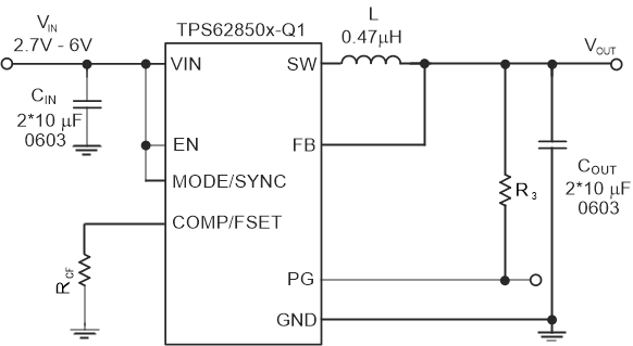
GUID-24B9F4F4-8E04-4901-AE8F-76565069BC41-low.gifFigure 9-57 Schematic for Fixed Output Voltage Versions