JAJSHB0 April   2019 TPS650002-Q1

PRODUCTION DATA.  

  1. 特長
  2. アプリケーション
  3. 概要
    1.     Device Images
      1.      代表的なアプリケーションの回路図
  4. 改訂履歴
  5. Pin Configuration and Functions
    1.     Pin Functions
  6. Specifications
    1. 6.1 Absolute Maximum Ratings
    2. 6.2 ESD Ratings
    3. 6.3 Recommended Operating Conditions
    4. 6.4 Thermal Information
    5. 6.5 Electrical Characteristics
    6. 6.6 Switching Characteristics
    7. 6.7 Typical Characteristics
  7. Detailed Description
    1. 7.1 Overview
    2. 7.2 Functional Block Diagram
    3. 7.3 Feature Description
      1. 7.3.1 Step-Down Converter
      2. 7.3.2 Soft Start
      3. 7.3.3 Linear Regulators
      4. 7.3.4 Power Good
    4. 7.4 Device Functional Modes
  8. Application and Implementation
    1. 8.1 Application Information
    2. 8.2 Typical Application
      1. 8.2.1 Design Requirements
      2. 8.2.2 Detailed Design Procedure
        1. 8.2.2.1 Output Filter Design (Inductor and Output Capacitor)
          1. 8.2.2.1.1 Inductor Selection
          2. 8.2.2.1.2 Output Capacitor Selection
        2. 8.2.2.2 Input Capacitor Selection
      3. 8.2.3 Application Curves
  9. Power Supply Recommendations
  10. 10Layout
    1. 10.1 Layout Guidelines
    2. 10.2 Layout Examples
  11. 11デバイスおよびドキュメントのサポート
    1. 11.1 デバイス・サポート
      1. 11.1.1 デベロッパー・ネットワークの製品に関する免責事項
    2. 11.2 ドキュメントのサポート
      1. 11.2.1 関連資料
    3. 11.3 ドキュメントの更新通知を受け取る方法
    4. 11.4 コミュニティ・リソース
    5. 11.5 商標
    6. 11.6 静電気放電に関する注意事項
    7. 11.7 Glossary
  12. 12メカニカル、パッケージ、および注文情報

パッケージ・オプション

メカニカル・データ(パッケージ|ピン)
サーマルパッド・メカニカル・データ
発注情報

Application Curves

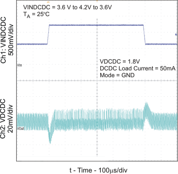
TPS650002-Q1 lt_dc_pfm_lvs810.gifFigure 22. Line Transient Response (DC-DC PFM Mode)
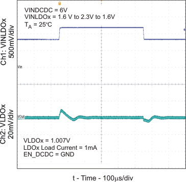
TPS650002-Q1 lt_ldo2_lvs810.gifFigure 24. Line Transient Response (LDOx)
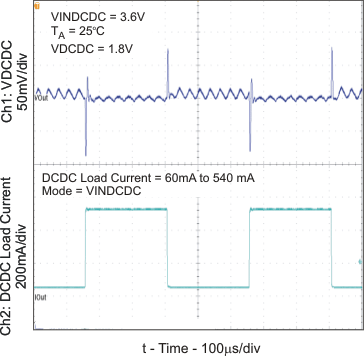
TPS650002-Q1 lt2_dc_pwm_lvs810.gifFigure 26. Load Transient Response (DC-DC PWM Mode)
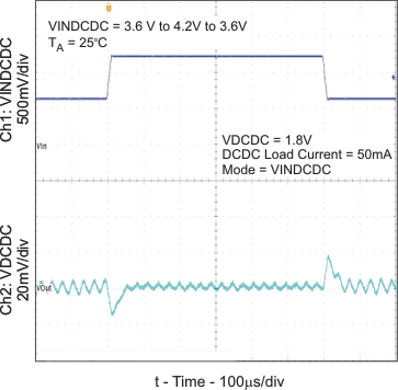
TPS650002-Q1 lt_dc_pwm_lvs810.gifFigure 23. Line Transient Response (DC-DC PWM Mode)
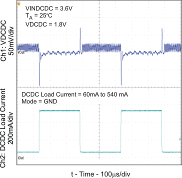
TPS650002-Q1 lt2_dc_pfm_lvs810.gifFigure 25. Load Transient Response (DC-DC PFM Mode)
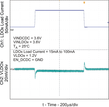
TPS650002-Q1 lt_ldo1_lvs810.gifFigure 27. Load Transient Response (LDOx)