SLVSAQ8G February 2011 – September 2017 TPS65185
PRODUCTION DATA.
- 1 Features
- 2 Applications
- 3 Description
- 4 Revision History
- 5 Description (continued)
- 6 Pin Configuration and Functions
- 7 Specifications
-
8 Detailed Description
- 8.1 Overview
- 8.2 Functional Block Diagram
- 8.3
Feature Description
- 8.3.1 Wake-Up and Power-Up Sequencing
- 8.3.2 Dependencies Between Rails
- 8.3.3 Soft Start
- 8.3.4 Active Discharge
- 8.3.5 VPOS/VNEG Supply Tracking
- 8.3.6 V3P3 Power Switch
- 8.3.7 VCOM Adjustment
- 8.3.8 Fault Handling And Recovery
- 8.3.9 Power Good Pin
- 8.3.10 Interrupt Pin
- 8.3.11 Panel Temperature Monitoring
- 8.4 Device Functional Modes
- 8.5 Programming
- 8.6
Register Maps
- 8.6.1 Thermistor Readout (TMST_VALUE) Register (address = 0x00h) [reset = N/A]
- 8.6.2 Enable (ENABLE) Register (address = 0x01h) [reset = 0h]
- 8.6.3 Voltage Adjustment (VADJ) Register (address = 0x02h) [reset = 23h]
- 8.6.4 VCOM 1 (VCOM1) Register (address = 0x03h) [reset = 7Dh]
- 8.6.5 VCOM 2 (VCOM2) Register (address = 0x04h) [reset = 04h]
- 8.6.6 Interrupt Enable 1 (INT_EN1) Register (address = 0x05h) [reset = 7Fh]
- 8.6.7 Interrupt Enable 2 (INT_EN2) Register (address = 0x06h) [reset = FFh]
- 8.6.8 Interrupt 1 (INT1) Register (address = 0x07h) [reset = 0h]
- 8.6.9 Interrupt 2 (INT2) Register (address = 0x08h) [reset = N/A]
- 8.6.10 Power-Up Sequence 0 (UPSEQ0) Register (address = 0x09h) [reset = E4h]
- 8.6.11 Power-Up Sequence 1 (UPSEQ1) Register (address = 0x0Ah) [reset = 55h]
- 8.6.12 Power-Down Sequence 0 (DWNSEQ0) Register (address = 0x0Bh) [reset = 1Eh]
- 8.6.13 Power-Down Sequence 1 (DWNSEQ1) Register (address = 0x0Ch) [reset = E0h]
- 8.6.14 Thermistor 1 (TMST1) Register (address = 0x0Dh) [reset = 20h]
- 8.6.15 Thermistor 2 (TMST2) Register (address = 0x0Eh) [reset = 78h]
- 8.6.16 Power Good Status (PG) Register (address = 0x0Fh) [reset = 0h]
- 8.6.17 Revision and Version Control (REVID) Register (address = 0x10h) [reset = 45h]
- 9 Application and Implementation
- 10Power Supply Recommendations
- 11Layout
- 12Device and Documentation Support
- 13Mechanical, Packaging, and Orderable Information
パッケージ・オプション
メカニカル・データ(パッケージ|ピン)
サーマルパッド・メカニカル・データ
発注情報
11 Layout
11.1 Layout Guidelines
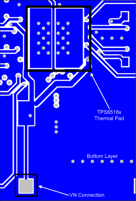
- PBKG (Die substrate) must connect to VN (–16 V) with short, wide trace. Wide copper trace will improve heat dissipation.
- The thermal pad is internally connected to PBKG and must not be connected to ground, but connected to VN with a short wide copper trace.
- Inductor traces must be kept on the PCB top layer free of any vias.
- Feedback traces must be routed away from any potential noise source to avoid coupling.
- Output caps must be placed immediately at output pin.
- The VIN pins must be bypassed to ground with low ESR ceramic bypass capacitors.
11.2 Layout Example
 Figure 51. Layout Diagram