SLVSD66 September 2015 TPS65233-1
PRODUCTION DATA.
- 1 Features
- 2 Applications
- 3 Description
- 4 Revision History
- 5 Pin Configuration and Functions
- 6 Specifications
- 7 Detailed Description
- 8 Application and Implementation
- 9 Power Supply Recommendations
- 10Layout
- 11Device and Documentation Support
- 12Mechanical, Packaging, and Orderable Information
パッケージ・オプション
メカニカル・データ(パッケージ|ピン)
- RTE|16
サーマルパッド・メカニカル・データ
- RTE|16
発注情報
7 Detailed Description
7.1 Overview
The TPS65233-1 is a power management IC that integrates a boost converter, a LDO, and a 22-kHz tone generator that serves as a LNB power supply. This solution compiles the DiSEqC 1.x standard with or without I2C interface. Output current can be precisely programmed by an external resistor. There are five ways to generate the 22-kHz tone signal with or without I2C. Integrated boost features low Rdson MOSFET and internal compensation. A fixed 1-MHz switching frequency is designed to reduce components size.
7.2 Functional Block Diagram
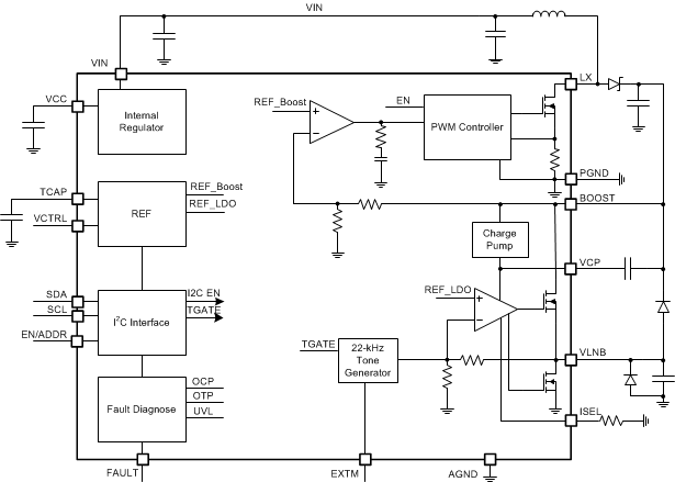
7.3 Feature Description
7.3.1 Boost Converter
The TPS65233-1 consists of an internal compensated boost converter and linear regulator. The boost converter tracks the output LNB voltage to within 800 mV even at loading 950 mA, to minimize power dissipation. Under conditions where the input voltage, VBOOST, is greater than the output voltage, VLNB, the linear regulator must drop the differential voltage. When operating in these conditions, taken care to ensure that the safe operating temperature range of the TPS65233-1 is not exceeded. The boost converter operates at 1 MHz typical. The TPS65233-1 has internal pulse-by-pulse current limiting on the boost converter and DC current limiting on the LNB output to protect the IC against short circuits. When the LNB output is shorted, the LNB output current is limited. The current limit is set by the external resistor. And the IC will be shut down if the overcurrent condition lasts for more than 4 ms, the converter enters hiccup mode and will retry startup in 128 ms. At extremely light loads, the boost converter operates in a pulse-skipping mode.
If two or more set top box LNB outputs are connected together, one output voltage could be set higher than others. The output with lower set voltage would be effectively turned off. Once the voltage drops to the set level, the LNB output with lower set output voltage will return to normal conditions.
7.3.2 Linear Regulator and Current Limit
The linear regulator is used to generate the 22-kHz tone signal by changing the reference voltage. The linear regulator features low drop out voltage to minimize power loss while keeping enough head room for the 0.68-V, 22-kHz tone. It also implements a tight current limit for over current protection. The current limit is set by an external resistor connected to the ISEL pin. The curve below shows the relationship between the current limit threshold and the resistor value.
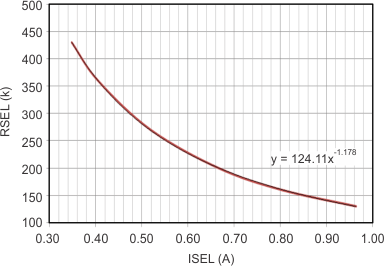 Figure 8. Linear Regulator Current Limit vs Resistor

A 280-kΩ resistor sets the current to 0.5 A. The current limit can also be set by I2C through a register.
7.3.3 Charge Pump
The charge pump circuitry generates a voltage to drive the NMOS of the linear regulator. One end the charge pump capacitor is connected to the output of the boost converter. The voltage on the charge pump capacitor is about 6.25 V.
7.3.4 Slew Rate Control
When LNB output voltage transits from 13 V to 18 V or vice versa, the capacitor at pin TCAP controls the transition time. This transition is to make sure the boost converter can follow the voltage change. Usually boost converter has low bandwidth and can’t response fast. The voltage at TCAP acts as the reference voltage of the linear regulator. The boost converter’s reference is also based on TCAP with additional fixed voltage to generate 0.8 V above the output.
The charging and discharging current is 10 µA, thus the transition time can be calculated as:

A 22-nF capacitor generates a 1.1-ms transition time.
In light load conditions, when LNB output voltage is set from 18 to 13 V, the voltage might drops very slow, which might cause wrong logic detection at LNB side. The TPS65233-1 has an integrated pull down circuit to pull down the output during the transition. This ensures the voltage change can follow the voltage at TCAP. Meanwhile, when the 22-kHz tone signal is superimposing on the LNB output voltage, the pull down current can also provide a square wave instead of distorted waveforms, which could cause another detection problem.
7.3.5 Short Circuit Protection, Hiccup, and Overtemperature Protection
The LNB output limit can be set by an external resistor. When short circuit conditions occur, the output current is clamped at the current limit for 4 ms. If the condition remains, the converter will shut down for 128 ms and then try restart. This hiccup behavior prevents the IC from overheating.
The low side MOSFET of the boost converter has a current limit threshold at 3.2 A, which serves as secondary protection. If the boost converter’s peak current limit is triggered, the peak current will clamp at 3.2 A. If loading current continues to increase, output voltage starts to drop and output power drops.
Thermal shutdown prevents the chip from operating at exceedingly high temperatures. When the silicon die temperature exceeds 160°C, the output shuts down. When the temperature drops below its lower threshold, typically 140°C, the output is enabled.
When the chip is in over current protection or thermal shutdown, the I2C interface and some logic are still active. The Fault pin is pulled down to signal the processor. The Fault pin signal will remain low unless the following actions are taken:
- If I2C interface is not used to control, Enable pin must be recycled in order to pull Fault pin back to high.
- If I2C interface is used, the I2C master needs to read the OCP or OTP bit in the register, then the Fault pin returns to high.
7.4 Device Functional Modes
7.4.1 Tone Generation
A 22-kHz tone signal is superimposed at the LNB output voltage as a carrier for DiSEqC command. This tone signal can be generated by feeding an external 22-kHz clock at the EXTM pin. It can also be generated with its internal tone generator gated by control logic. The output stage of the regulator facilitates a push-pull circuit, so even at zero loading the 22-kHz tone at the output is still clear of distortion.
There are five ways to generate the 22-kHz tone signal at the output.
In non-I2C mode, only option 1 and option 2 are supported in TPS65233-1. EXTM can be tone envelope or 22 kHz burst pulse as shown in Figure 9. Option 3 and option 4 are designed for I2C interface communication mode. In I2C communication mode, TGATE bit must be written through I2C bus. If there is no bandwidth of I2C bus to write TGATE bit, there is a supplemental option 5 to generate 22-kHz tone, as shown in Figure 10. In option 5, bit TMODE and TGATE must be set as 1.
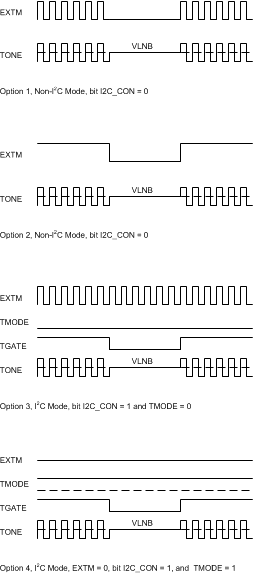 Figure 9. Four Ways to Generate 22-kHz Tone
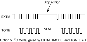 Figure 10. Supplemental Option for 22-kHz Tone in I2C Mode
7.4.2 Serial Interface
I2C is a 2-wire serial interface developed by Philips Semiconductor (see I2C-Bus Specification, Version 2.1, January 2000). The bus consists of a data line (SDA) and a clock line (SCL) with pull-up structures. When the bus is idle, both SDA and SCL lines are pulled high. All the I2C compatible devices connect to the I2C bus through open drain I/O pins, SDA and SCL. A master device, usually a microcontroller or a digital signal processor, controls the bus. The master is responsible for generating the SCL signal and device addresses. The master also generates specific conditions that indicate the START and STOP of data transfer. A slave device receives and transmits data on the bus under control of the master device.
The TPS65233-1 device works as a slave and supports the following data transfer modes, as defined in the I2C-Bus Specification: standard mode (100 kbps), and fast mode (400 kbps). The interface adds flexibility to the power supply solution, enabling most functions to be programmed to new values depending on the instantaneous application requirements. Register contents remain intact as long as supply voltage remains above 4.5 V (typical).
The data transfer protocol for standard and fast modes is exactly the same; therefore, they are referred to as F/S-mode in this document. The TPS65233-1 device supports 7-bit addressing; 10-bit addressing and general call address are not supported.
The TPS65233-1 device has a 7-bit address with the 2 LSB bits set by EN pin. Connecting EN to ground set the address 0x60H, connecting to high set the address 0x61H.
Table 1. I2C Address Selection
| EN/ADDR PIN | I2C ADDRESS | ADDRESS FORMAT (A6...A0) |
|---|---|---|
| Connect to ground | 0x60H | 110 0000 |
| Connect to high | 0x61H | 110 0001 |
7.5 Programming
7.5.1 I2C Update Sequence
The TPS65233-1 requires a start condition, a valid I2C address, a register address byte, and a data byte for a single update. After the receipt of each byte, the TPS65233-1 device acknowledges by pulling the SDA line low during the high period of a single clock pulse. The TPS65233-1 performs an update on the falling edge of the LSB byte.
When the TPS65233-1 is disabled (EN pin tied to ground) the device can still be updated via the I2C interface.
 Figure 11. I2C Write Data Format
 Figure 12. I2C Read Data Format
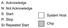 Figure 13. Legend
7.6 Register Map
The registers are listed in Table 2 and described in the following sections.
Table 2. Register Map
| REGISTER / ADDRESS | 7 | 6 | 5 | 4 | 3 | 2 | 1 | 0 |
|---|---|---|---|---|---|---|---|---|
| Control Register 1 Address: 0x00H | I2C_CON | Reserved | TGATE | TMODE | EN | VSEL2 | VSEL1 | VSEL0 |
| Control Register 2 Address: 0x01H | — | — | — | TONE_ POS1 |
TONE_ POS0 |
CL1 | CL0 | CL_EXT |
| Status Register 1 Address: 0x02H | — | T125 | LDO_ON | Reserved | TSD | OCP | CABLE_ GOOD |
VOUT_ GOOD |
7.6.1 Control Register 1 - Address: 0x00H
Table 3. Control Register 1 - Address: 0x00H
| BIT | FIELD | TYPE | RESET | DESCRIPTION |
|---|---|---|---|---|
| 7 | I2C_CON | R/W | 0 | 1: I2C control enabled; 0: I2C control disabled |
| 6 | Reserved | R/W | 0 | Reserved |
| 5 | TGATE | R/W | 0 | Tone Gate. Allows either the internal or external 22-kHz tone signals to be gated. 1: Tone Gate on use; 0: Tone gate off |
| 4 | TMODE | R/W | 0 | Tone mode. Select between the use of an external 22-kHz or internal 22-kHz signal. 1: internal; 0: external |
| 3 | EN | R/W | 1 | LNB output voltage Enable 1: output enabled; 0: output disabled |
| 2 | VSEL2 | R/W | 0 | See Table 4 for output voltage selection |
| 1 | VSEL1 | R/W | 0 | |
| 0 | VSEL0 | R/W | 0 |
Table 4. Voltage Selection Bits
| VSEL2 | VSEL1 | VSEL0 | LNB(V) |
|---|---|---|---|
| 0 | 0 | 0 | 13 |
| 0 | 0 | 1 | 13.4 |
| 0 | 1 | 0 | 13.8 |
| 0 | 1 | 1 | 14.2 |
| 1 | 0 | 0 | 18 |
| 1 | 0 | 1 | 18.6 |
| 1 | 1 | 0 | 19.2 |
| 1 | 1 | 1 | 19.8 |
7.6.2 Control Register 2 - Address: 0x01H
Table 5. Control Register 2 - Address: 0x01H
| BIT | FIELD | TYPE | RESET | DESCRIPTION |
|---|---|---|---|---|
| 7 | — | R/W | — | — |
| 6 | — | R/W | — | — |
| 5 | — | R/W | — | — |
| 4 | TONE_POS1 | R/W | 0 | 00: tone above Vout; 01: tone in the middle of Vout; 10: tone below Vout |
| 3 | TONE_POS0 | R/W | 1 | |
| 2 | CL1 | R/W | 0 | Current limit set bits |
| 1 | CL0 | R/W | 0 | |
| 0 | CL_EXT | R/W | 1 | 1: current limit set by external resistor; 0: current limit set by register |
Some tone detection circuits in LNB are sensitive to the position of the tone on the output voltage. The TPS65233-1 provides options to select the position by setting the TONE_POS1 and TONE_POS0 bits, as illustrated below.
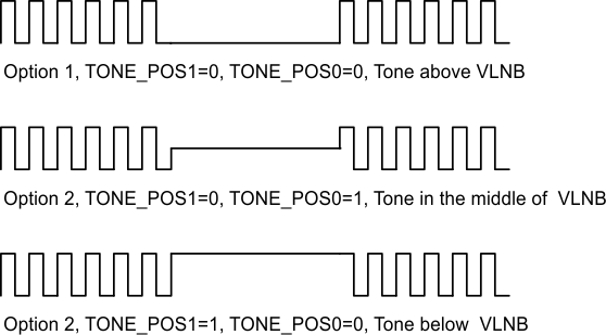 Figure 14. Tone Position Programmed by TONE_POS1, TONE_POS0 Bits
In addition to programming the LDO’s current continuously via an external resistor, internal registers also provide options to program the current limit. There are four options that can be selected.
Table 6. Current Limit Selection Bits
| CL1 | CL0 | CURRENT LIMIT (mA) |
|---|---|---|
| 0 | 0 | 400 |
| 0 | 1 | 600 |
| 1 | 0 | 750 |
| 1 | 1 | 1000 |
7.6.3 Status Register 1 - Address: 0x02H
The TPS65233-1 has a full range of diagnostic flags for operation and debug. If any of the flags are triggered, the FAULT pin is pulled low sending an interrupt signal to processor. The processor then can read the status register to check the error conditions. The status bits are described in the following table. Among these bits, TSD and OCP are different from the others. Once TSD and OCP are set to 1, the FAULT pin logic is latched low and the processor must reset the bits in order to release the fault conditions. Other bits change as conditions change without latch.
Table 7. Status Register 1 - Address: 0x02H
| BIT | FIELD | TYPE | RESET | DESCRIPTION |
|---|---|---|---|---|
| 7 | — | — | — | — |
| 6 | T125 | R | 0 | 1: if die temperature T > 125°C; 0: if die temperature T < 125°C |
| 5 | LDO_ON | R | 0 | 1: internal LDO is turned on and boost converter is on; 0: Internal LDO is turned off but boost converter is on |
| 4 | Reserved | R | 0 | Reserved |
| 3 | TSD | R | 0 | 1: thermal shutdown occurs; 0: thermal shutdown does not occur. FAULT pin pull low and latch, I2C master need to read and release |
| 2 | OCP | R | 0 | Overcurrent protection. If over current conditions last for more than 48 ms. 1: Overcurrent protection triggered. 0: Overcurrent protection conditions released. FAULT pin pull low and latch, I2C master need to read and release |
| 1 | CABLE_GOOD | R | 0 | Cable connection good. 1: Output current above 50 mA; 0: Output current less than 50 mA |
| 0 | VOUT_GOOD | R | 0 | LNB output voltage in range. 1: In range; 0: Out of range |