JAJSC02C december 2013 – may 2023 TPS65261 , TPS65261-1
PRODUCTION DATA
- 1
- 1 特長
- 2 アプリケーション
- 3 概要
- 4 Revision History
- 5 Pin Configuration and Functions
- 6 Specifications
-
7 Detailed Description
- 7.1 Overview
- 7.2 Functional Block Diagram
- 7.3
Feature Description
- 7.3.1 Adjusting the Output Voltage
- 7.3.2 Power Failure Detector
- 7.3.3 Enable and Adjusting Undervoltage Lockout
- 7.3.4 Soft-Start Time
- 7.3.5 Power Up Sequencing
- 7.3.6 V7V Low Dropout Regulator and Bootstrap
- 7.3.7 Out-of-Phase Operation
- 7.3.8 Output Overvoltage Protection (OVP)
- 7.3.9 Slope Compensation
- 7.3.10 Overcurrent Protection
- 7.3.11 Power Good
- 7.3.12 Adjustable Switching Frequency
- 7.3.13 Thermal Shutdown
- 7.4 Device Functional Modes
- 8 Application and Implementation
- 9 Device and Documentation Support
- 10Mechanical, Packaging, and Orderable Information
パッケージ・オプション
メカニカル・データ(パッケージ|ピン)
- RHB|32
サーマルパッド・メカニカル・データ
- RHB|32
発注情報
7.3.2 Power Failure Detector
The power failure detector monitors the voltage on VDIV, and sets open-drain output RESET low when VDIV is below 1.23V. There is deglitch on the rising edge, 534 frequency cycles. Figure 7-2 shows the power failure detector timing diagram.
 Figure 7-2 Power Failure Detector Timing Diagram
The thresholds can be calculated using Equation 2 and Equation 3.
Equation 2. 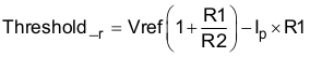
Equation 3. 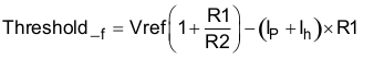
The divider resisters can be calculated using Equation 4 and Equation 5.
Equation 4. 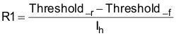
Equation 5. 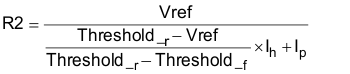
Where Ih = 1µA, Ip = 1µA.