JAJSQ69B december 2015 – may 2023 TPS65265
PRODUCTION DATA
- 1
- 1 特長
- 2 アプリケーション
- 3 概要
- 4 Revision History
- 5 Device Comparison Table
- 6 Pin Configuration and Functions
- 7 Specifications
-
8 Detailed Description
- 8.1 Overview
- 8.2 Functional Block Diagram
- 8.3
Feature Description
- 8.3.1 Adjusting the Output Voltage
- 8.3.2 Mix PGOOD, PG_DLY Functions
- 8.3.3 Enable and Adjusting UVLO
- 8.3.4 Soft-Start Time
- 8.3.5 Power-Up Sequencing
- 8.3.6 V7V Low Dropout Regulator and Bootstrap
- 8.3.7 Out of Phase Operation
- 8.3.8 Output Overvoltage Protection (OVP)
- 8.3.9 PSM
- 8.3.10 Slope Compensation
- 8.3.11 Overcurrent Protection
- 8.3.12 Adjustable Switching Frequency
- 8.3.13 Thermal Shutdown
- 8.4 Device Functional Modes
- 9 Application and Implementation
- 10Device and Documentation Support
- 11Mechanical, Packaging, and Orderable Information
パッケージ・オプション
メカニカル・データ(パッケージ|ピン)
- RHB|32
サーマルパッド・メカニカル・データ
- RHB|32
発注情報
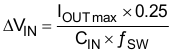
9.2.2.3 Input Capacitor Selection
The TPS65265 requires a high quality ceramic, type X5R or X7R, input decoupling capacitor of at least 10 µF of effective capacitance on the PVIN input voltage pins. In some applications additional bulk capacitance can also be required for the PVIN input. The effective capacitance includes any DC bias effects. The voltage rating of the input capacitor must be greater than the maximum input voltage. The capacitor must also have a ripple current rating greater than the maximum input current ripple of The TPS65265. The input ripple current can be calculated using Equation 17.
The value of a ceramic capacitor varies significantly over temperature and the amount of DC bias applied to the capacitor. The capacitance variations due to temperature can be minimized by selecting a dielectric material that is stable over temperature. X5R and X7R ceramic dielectrics are usually selected for power regulator capacitors because they have a high capacitance to volume ratio and are fairly stable over temperature. The output capacitor must also be selected with the DC bias taken into account. The capacitance value of a capacitor decreases as the DC bias across a capacitor increases. The input capacitance value determines the input ripple voltage of the regulator. The input voltage ripple can be calculated using Equation 18.