SWCS048G March 2010 – September 2014 TPS65921
PRODUCTION DATA.
- 1Device Overview
- 2Revision History
- 3Terminal Configuration and Functions
-
4Specifications
- 4.1 Absolute Maximum Ratings
- 4.2 Handling Ratings
- 4.3 Recommended Operating Conditions
- 4.4 Thermal Resistance Characteristics for ZQZ Package
- 4.5 Crystal Oscillator
- 4.6 Clock Slicer
- 4.7 32KCLKOUT Output Clock
- 4.8 HFCLKOUT Output Clock
- 4.9 VDD1 DC-DC Converter
- 4.10 VDD2 DC-DC Converter
- 4.11 VIO DC-DC Converter
- 4.12 VMMC1 Low Dropout Regulator
- 4.13 VDAC Low Dropout Regulator
- 4.14 VAUX2 Low Dropout Regulator
- 4.15 VPLL1 Low Dropout Regulator
- 4.16 Internal LDOs
- 4.17 Voltage References
- 4.18 Battery Threshold Levels
- 4.19 Power Consumption
- 4.20 USB Charge Pump
- 4.21 Hot-Die Detection and Thermal Shutdown
- 4.22 USB
- 4.23 MADC
- 4.24 TPS65921 Interface Target Frequencies
- 4.25 JTAG Interfaces
- 5Detailed Description
- 6Device and Documentation Support
- 7Mechanical Packaging and Orderable Information
パッケージ・オプション
メカニカル・データ(パッケージ|ピン)
サーマルパッド・メカニカル・データ
発注情報
5 Detailed Description
5.1 Functional Block Diagram
Figure 5-1 shows the functional block diagram of the device.
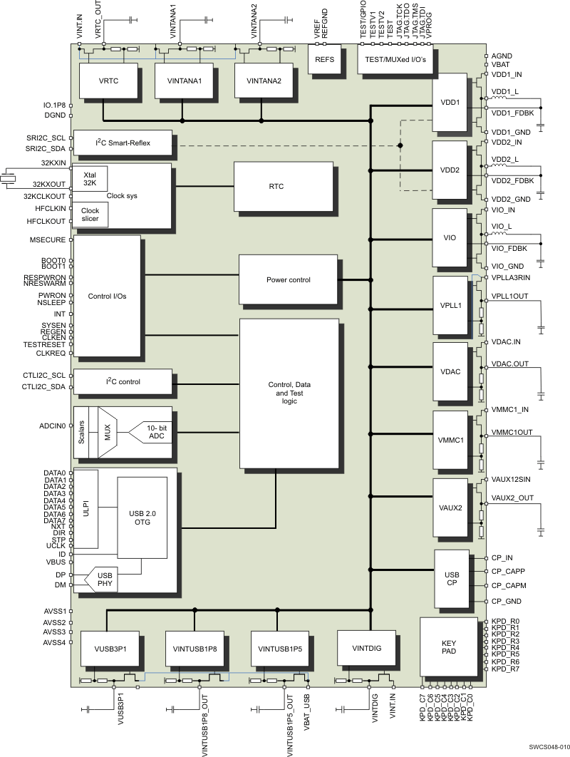 Figure 5-1 Functional Block Diagram
5.2 Clock System
Figure 5-2 shows the TPS65921 clock overview.
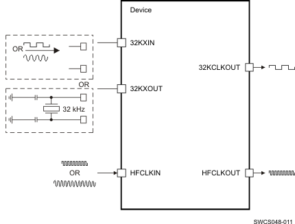 Figure 5-2 TPS65921 Clock Overview
The TPS65921 accepts two sources of high-stability clock signals:
- 32KXIN/32KXOUT: on-board 32-kHz crystal oscillator (optionally, an external 32-kHz input clock can be provided)
- HFCLKIN: an external high-frequency clock (19.2, 26, or 38.4 MHz)
The TPS65921 has the capability to provide:
- 32KCLKOUT digital output clock
- HFCLKOUT digital output clock with the same frequency as HFCLKIN input clock
5.3 32-kHz Oscillator
It is possible to use the 32-kHz input clock with either an external crystal or clock source. There are four configuration, one with the external crystal and three without.
- An external 32.768-kHz crystal connected on the 32KXIN / 32KXOUT balls. This configuration is available for the master mode only.
- A square- or sine-wave input can be applied to the 32KXIN pin with amplitude of 1.85 or 1.8 V. The 32KXOUT pin can be driven to a dc value of the square- or sine-wave amplitude divided by 2. This configuration is recommended if a large load is applied on the 32KXOUT pin.
- A square- or sine-wave input can be applied to the 32KXIN pin with amplitude of 1.85 or 1.8 V. The 32KXOUT pin can be left floating. This configuration is used if no charge is applied on the 32KXOUT pin.
- The oscillator is in bypass mode and a square-wave input can be applied to the 32KXIN pin with amplitude of 1.8 V. The 32KXOUT pin can be left floating. This configuration is used if the oscillator is in bypass mode (default configuration in Slave mode).
Figure 5-3 shows the block diagram for the 32.768-kHz clock output.
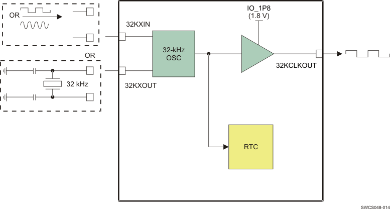 Figure 5-3 32.768-kHz Clock Output Block Diagram
The TPS65921 device has an internal 32.768-kHz oscillator connected to an external 32.768-kHz crystal through the 32KXIN/32KXOUT balls or an external digital 32.768-kHz clock through the 32KXIN input (see Figure 5-3). The TPS65921 device also generates a 32.768-kHz digital clock through the 32KCLKOUT pin and can broadcast it externally to the application processor or any other devices. The 32KCLKOUT clock is broadcast by default in the TPS65921 active mode but can be disabled if it is not used.
The 32.768-kHz clock (or signal) is also used to clock the RTC (real-time clock) embedded in the TPS65921. The RTC is not enabled by default. It is up to the host processor to set the correct date and time and to enable the RTC functionality.
The 32KCLKOUT output buffer can drive several devices (up to 40-pF load). At start-up, the 32.768-kHz output clock (32KCLKOUT) must be stabilized (frequency/duty cycle) prior to the signal output. Depending on the start-up condition, this may delay the start-up sequence.
5.4 Clock Slicer
Figure 5-4 shows the clock slicer block diagram.
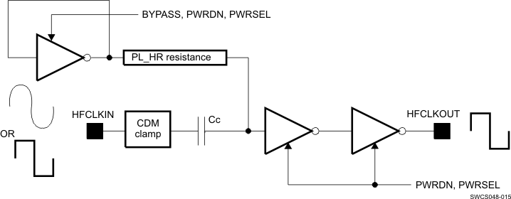 Figure 5-4 Clock Slicer Block Diagram
The clock slicer is disabled by default and enabled when the CLKEN pad is high. The slicer transforms the HFCLKIN clock input signal into a squared clock signal used internally by the TPS65921 device and also outputs it for external use. The HFCLKIN input signal can be:
- A sinusoid with peak-to-peak amplitude varying from 0.3 to 1.45 V
- A square clock signal of amplitude 1.85 V maximum. In the case of a square clock signal, the slicer is configured in bypass or power-down mode. If a square-wave input clock is provided, it is recommended to switch the block to bypass mode when possible to avoid loading the clock.
The HFCLKIN input clock frequency must be 19.2, 26, or 38.4 MHz.
Four different modes are programmable by register. By default, the slicer is in high-performance application mode:
- Bypass mode (BP): In BP mode, which overrides all the other modes, the input signal is directly connected to the output through some buffers. The input is a rail-to-rail square wave.
- Power-down mode (PD): During PD mode, the cell does not consume any current if bypass mode is not active.
- Low-power application mode (LP): In LP mode, the input sine wave is converted to a CMOS signal (square wave) with low power consumption.
- High-performance application mode (HP): In HP mode, the input sine wave is converted to a CMOS signal (square wave). It has lower duty cycle degradation and lower input-to-output delay in comparison to the low-power mode, but it consumes more current. The drive of the squaring inverter is increased by connecting additional inverters in parallel. Details can be found in the clock slicer electrical characteristics table.
Figure 5-5 shows the HFCLKIN clock distribution.
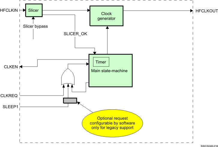 Figure 5-5 HFCLKIN Clock Distribution
When a device needs a clock signal other than 32.768 kHz, it makes a clock request and activates the CLKREQ pin. As a result, the TPS65921 device immediately sets CLKEN to 1 to warn the clock provider in the system about the clock request and starts a timer (maximum of 10 ms and uses the 32.768-kHz clock). Once the timer expires, the TPS65921 device opens a gated clock, the timer automatically reloads the defined value and a high-frequency output clock signal is available through the HFCLKOUT pin. The output drive of HFCLKOUT is programmable (low drive (MISC_CFG[CLK_HF_DRV] = 0) maximum load 20 pF, high drive (MISC_CFG[CLK_HF_DRV] = 1) maximum load 30 pF), by default it is programmed to support Low Drive.
CLKREQ, when enabled, has a weak pulldown resistor to support the wired-OR clock request.
Figure 5-6 shows an example of the wired-OR clock request.
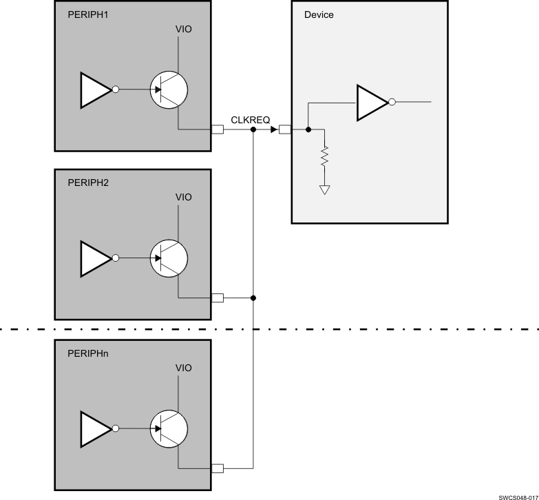 Figure 5-6 Example of Wired-OR Clock Request
The timer default value must be the worst case (10 ms) for the clock providers. For legacy or workaround support, the NSLEEP1 signal can also be used as a clock request even if it is not its primary goal. By default, this feature is disabled and must be enabled individually by setting the register bits associated with each signal.
5.5 Power Path
5.5.1 Step-Down Converters
Depending on the system requirements, and also to optimize mean consumption, three operating modes are allowed for each step-down converter:
- Off/power-down mode: Output voltage is not maintained, and power consumption is null
- Active: DC-DC can deliver its nominal output voltage with a full load current capability.
- Sleep: The nominal output voltage is maintained with low power consumption, but also with a low load-current capability.
The SMPS operates with three modulation schemes:
- Light pulse frequency modulation (PFM)
- Pulse skipping mode (PSM)
- Continuous pulse-width modulation (PWM)
Each DC-DC converter, all of which have the same electrical characteristics, has an integrated RC oscillator. The use of these RC oscillators is configurable through register bits, and by default the RC oscillator of VDD1 is used for all DC-DC converters.
5.5.2 LDO
The VPLL1 programmable LDO regulator is high-PSRR, low-noise, linear regulator used for the host processor PLL supply.
The VDAC programmable LDO regulator is a high-PSRR, low-noise, linear regulator that powers the host processor dual-video DAC. It is controllable with registers through I2C and can be powered down.
The VMMC1 LDO regulator is a programmable linear voltage converter that powers the MMC slot. It includes a discharge resistor and over-current protection (short circuit). This LDO regulator can also be turned off automatically when the MMC card extraction is detected (through one dedicated GPIO). The VMMC1 LDO can be powered through an independent supply other than the battery; for example, a charge pump. In this case, the input from the VMMC1 LDO can possibly be higher than the battery voltage.
The VAUX2 general-purpose LDO regulator powers the auxiliary devices.
The VRRTC voltage regulator is a programmable, LDO, linear voltage regulator supplying (1.5 V) the embedded RTC (32.768-kHz oscillator) and dedicated I/Os of the digital host counterpart. The VRRTC regulator is also the supply voltage of the power-management digital state-machine. The VRRTC regulator is supplied from the UPR line, switched on by the main battery. The VRRTC output is present as long as a valid energy source is present. The VRRTC line is supplied by an LDO when VBAT > 2.7 V, and a clamp circuit when VBAT < 2.7 V.
The VINTDIG LDO regulator supplies the TPS65921 digital blocks.
To supply the TPS65921 analog blocks, there are two LDOs: VINTANA1 (1.5 V) and VINTANA2 (2.75 V/2.5 V). The 2.5-V setting is selected when the battery voltage falls below 3.0 V.
The VUSB3V1 internal LDO regulator powers the USB PHY, charger detection, and OTG of the USB subchip inside the TPS65921 device.
It can take its power from two possible sources:
- VBAT.USB (only for high battery voltages)
- VBUS (only in low-power mode)
See Charge-pump section for more details.
The USB standard requires data lines to be biased with pullups biased from a > 3.0 V supply, USB PHY cannot directly operate from VBAT.USB for battery voltages lower than 3.3 V.
In such case, VBUS should be supplied by a boosted voltage to ensure enough overhead for USB LDO operation. An internal charge pump (whose output is connected to VBUS) can be used for this purpose.
To select between these two power sources, a power mux is connected to the VUSB3V1 LDO supply.
The VUSB1V8 and VUSB1V5 internal LDO regulators power the USB subchip inside the TPS65921 device.
The short-circuit current for the LDOs and DC-DCs in the TPS65921 device is approximately twice the maximum load current. In certain cases when the output of the block is shorted to ground, the power dissipation can exceed the 1.2 W requirement if no action is taken. A short-circuit protection scheme is included in the TPS65921 device to ensure that if the output of an LDO or DC-DC converter is short-circuited, then the power dissipation does not exceed the 1.2-W level.
The three USB LDOs VUSB3V1, VUSB1V8, and VUSB1V5 are included in this short circuit protection scheme which monitors the LDO output voltage at a frequency of 1 Hz, and generates an interrupt when a short circuit is detected.
The scheme compares the LDO output voltage to a reference voltage and detects a short circuit if the LDO voltage drops below this reference value (0.5 V or 0.75 V programmable). In the case of the VUSB3V1 and VUSB1V8 LDOs, the reference is compared with a divided down voltage (1.5 V typical).
If a short circuit is detected on VUSB3V1, then the power subchip FSM switches this LDO to sleep-mode.
If a short circuit is detected on VUSB1V8 or VUSB1V5, then the power subchip FSM switches the relevant LDO off.
5.5.3 Power Reference
The bandgap voltage reference is filtered (RC filter), using an external capacitor connected across the VREF output and an analog ground (REFGND). The VREF voltage is scaled, distributed, and buffered inside the device. The bandgap is started in fast mode (not filtered) and is set automatically by the power state-machine in slow mode (filtered, less noisy) after switch on.
5.5.4 Power Use Cases
The TPS65921 device has two modes:
- Master: The TPS65921 device decides to power up or down the system and control the other power ICs in the system with the SYSEN output.
- Slave: The TPS65921 device is controlled by another power IC with a digital signal on the PWRON input. There is no battery management in slave mode.
The modes corresponding to BOOT0–BOOT1 combination value are:
| NAME | DESCRIPTION | BOOT0 | BOOT1 |
|---|---|---|---|
| MC021(1) | Master_C021_Generic 10 | 1 | 0 |
| SC021 | Slave_C021_Generic 11 | 1 | 1 |
Process modes define:
- The boot voltage for the host core
- The boot sequence associated with the process
- The DVFS protocol associated with the process
| MODE | C021.M |
|---|---|
| Boot core voltage | 1.2 V |
| Power sequence | VIO followed by VPLL1, VDD2, VDD1 |
| DVFS protocol | SmartReflex interface (I2C high speed) |
Regulator states depending on use cases:
| REGULATOR | MODE: C021 (MASTER/SLAVE) | |||
|---|---|---|---|---|
| BACKUP | WAIT ON | SLEEP NO LOAD | ACTIVE NO LOAD | |
| VAUX2 | OFF | OFF | OFF | OFF |
| VMMC1 | OFF | OFF | OFF | OFF |
| VPLL1 | OFF | OFF | SLEEP | ON |
| VDAC | OFF | OFF | OFF | OFF |
| VINTANA1 | OFF | OFF | SLEEP | ON |
| VINTANA2 | OFF | OFF | SLEEP | ON |
| VINTDIG | OFF | OFF | SLEEP | ON |
| VIO | OFF | OFF | SLEEP | ON |
| VDD1 | OFF | OFF | SLEEP | ON |
| VDD2 | OFF | OFF | SLEEP | ON |
| VUSB1V5 | OFF | OFF | OFF | OFF |
| VUSB1V8 | OFF | OFF | OFF | OFF |
| VUSB3V1 | OFF | OFF | SLEEP | ON |
5.5.5 Power Timing
Sequence start is a symbolic internal signal to ease the description of the power sequences and occurs according to the different events detailed in Figure 5-7.
Sequence start timing depends on the TPS65921 starting event. If the starting event is:
- Main battery insertion, event time is 1.126 ms (time to set up internal LDO and relax internal reset)
- VBUS insertion, event time is 25 cycles of 32k
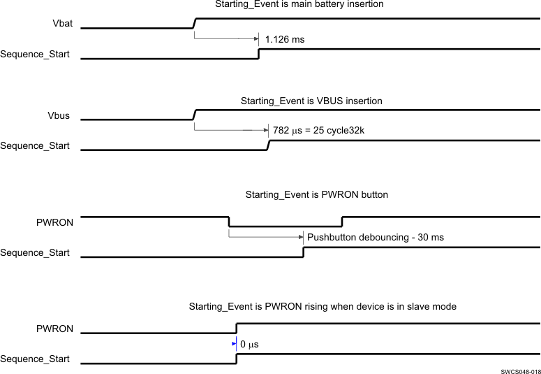 Figure 5-7 Timings Before Sequence Start
5.5.5.1 Switch On In MASTER_C021_GENERIC Mode
Figure 5-8 describes the timing and control that must occur in Master_C021_Generic mode. Sequence_Start is a symbolic internal signal to ease the description of the power sequences and occurs according to the different events detailed in Figure 5-7.
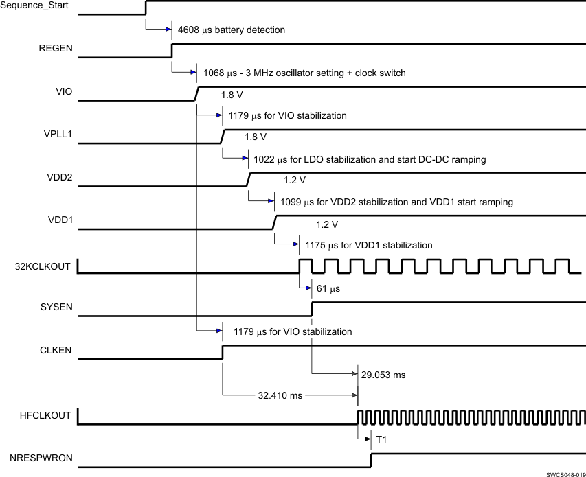 Figure 5-8 Timings—Switch On in Master_C021_Generic Mode
| PARAMETER | MIN | MAX | UNIT | |
|---|---|---|---|---|
| T1 | 10 | 11 | 32k clock cycles | |
5.5.5.2 Switch On In SLAVE_C021_GENERIC Mode
Figure 5-9 describes the timing and control that must occur in Slave_C021_Generic mode. Sequence_Start is a symbolic internal signal to ease the description of the power sequences and occurs according to the different events detailed in Figure 5-7.
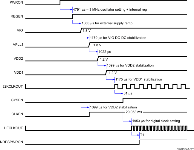 Figure 5-9 Timings—Switch On in Slave_C021_Generic Model
| PARAMETER | MIN | MAX | UNIT | |
|---|---|---|---|---|
| T1 | 10 | 11 | 32k clock cycles | |
5.5.5.3 Switch-Off Sequence
This section describes the signal behavior required to switch off the system.
5.5.5.3.1 Switch-Off Sequence In Master Modes
Figure 5-10 describes the timing and control that occur during the switch-off sequence in master modes.
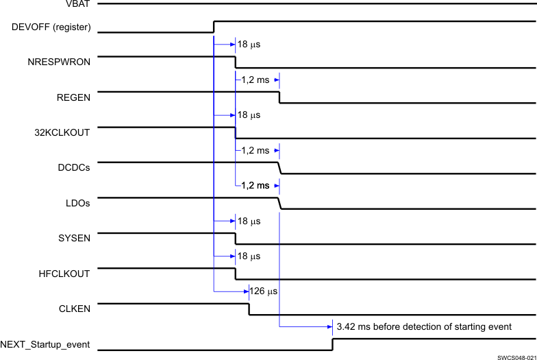
In case the value of the HF clock is different from 19.2 MHz (with HFCLK_FREQ bit field values set accordingly inside the CFG_BOOT register), then the delay between DEVOFF and NRESPWRON/CLK32KOUT/SYSEN/HFCLKOUT is divided by 2 (meaning around 9 μs). This is due to the internal frequency used by POWER STM switching from 3 MHz to 1.5 MHz in case the value of the HF clock is 19.2 MHz.
The DEVOFF event is the PWRON falling edge in slave mode and the DEVOFF internal register write in master mode.
5.5.5.3.2 Switch-Off Sequence in Slave Mode
Figure 5-11 describes the timing and control that occur during the switch off-sequence in slave mode.
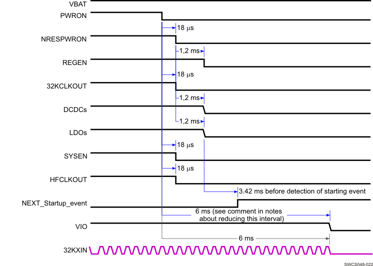
If necessary, the 6-ms period to maintain VIO and 32KXIN after PWRON goes low can be reduced to 150 μs.
In case the value of the HF clock is different from 19.2 MHz (with HFCLK_FREQ bit field values set accordingly inside the CFG_BOOT register), then the delay between DEVOFF and NRESPWRON/CLK32KOUT/ SYSEN/HFCLKOUT is divided by 2 (meaning around 9 μs). This is due to the internal frequency used by POWER STM switching from 3 MHz into 1.5 MHz in case the value of the HF clock is 19.2 MHz.
5.5.5.4 Charge Pump
The charge pump generates a 5.0-V (nominal) power supply voltage from battery to the VBUS CP.OUT/VUSB.IN pin. The input voltage range is 2.7 to 4.5 V for the battery voltage. The charge pump operating frequency is 1 MHz.
The charge pump tolerates 6 V on VBUS when it is in power down mode. The charge pump integrates a short-circuit current limitation at 450 mA.
Figure 5-12 shows the charge pump.
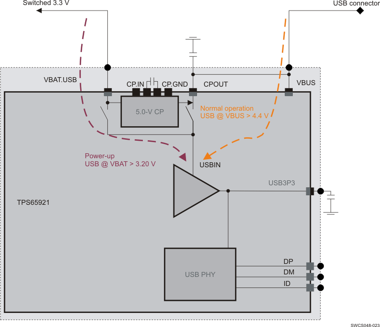 Figure 5-12 General Overview of the Charge Pump and Its Interfaces
The charge pump can be used to supply USB 3.1 V LDO when battery voltage is lower than this LDO VBATmin voltage (see Section 4).
5.5.6 USB Transceiver
The TPS65921 device includes a USB OTG transceiver that support USB 480 Mbps HS, 12 Mbps FS, and USB 1.5 Mbps LS through a 4-pin UTMI+ ULPI.
It also includes a module covering Battery Charging Specification v1.0. Figure 5-13 shows the USB 2.0 PHY highlight block diagram.
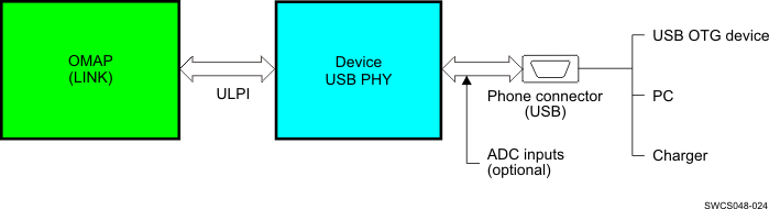 Figure 5-13 USB 2.0 PHY Highlight
Figure 5-14 shows the USB system application schematic.
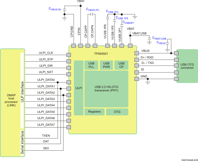 Figure 5-14 USB System Application Schematic
5.5.7 PHY
The PHY is the physical signaling layer of the USB 2.0. It contains all the drivers and receivers required for physical data and protocol signaling on the DP and DM lines.
The PHY interfaces to the USB controller through a standard digital interface called the universal transceiver macro cell interface (UTMI).
The transmitters and receivers inside the PHY are classified into two main classes:
- The FS and LS transceivers. These are the legacy USB1.x transceivers.
- The HS transceivers
To bias the transistors and run the logic, the PHY also contains reference generation circuitry consisting of:
- A DPLL, which does a frequency multiplication to achieve the 480-MHz low-jitter lock necessary for USB, and also the clock required for the switched capacitor resistance block.
- A switched capacitor resistance block used to replicate an external resistor on chip.
Built-in pullup and pulldown resistors are used as part of the protocol signaling.
Apart from this, the PHY also contains circuitry that protects it from an accidental 5 V short on the DP and DM lines.
5.5.7.1 LS/FS Single-Ended Receivers
In addition to the differential receiver, there is a single-ended receiver (SE–, SE+) for each of the two data lines D+/–. The main purpose of the single-ended receivers is to qualify the D+ and D– signals in the FS/LS modes of operation.
5.5.7.2 LS/FS Differential Receiver
A differential input receiver (RX) retrieves the LS/FS differential data signaling. The differential voltage on the line is converted into digital data by a differential comparator on DP/DM. This data is then sent to a clock and data recovery circuit, which recovers the clock from the data. In an additional serial mode, the differential data is directly output on the RXRCV pin.
5.5.7.3 LS/FS Transmitter
The USB transceiver (TX) uses a differential output driver to drive the USB data signal D+/– onto the USB cable. The outputs of the driver support 3-state operation to achieve bidirectional half-duplex transactions.
5.5.7.4 HS Differential Receiver
The HS receiver consists of the following blocks:
- A differential input comparator to receive the serial data
- A squelch detector to qualify the received data
- An oversampler-based clock data recovery scheme followed by a NRZI decoder, bit unstuffing, and serial-to-parallel converter to generate the UTMI DATAOUT
5.5.7.5 HS Differential Transmitter
The HS transmitter is always operated on the UTMI parallel interface. The parallel data on the interface is serialized, bit-stuffed, NRZI-encoded, and transmitted as a DC output current on DP or DM depending on the data. Each line has an effective 22.5-Ω load to ground, which generates the voltage levels for signaling.
A disconnect detector is also part of the HS transmitter. A disconnect on the far end of the cable causes the impedance seen by the transmitter to double, thereby doubling the differential amplitude seen on the DP and DM lines.
5.5.7.6 UART Transceiver
In this mode, the ULPI data bus is redefined as a 2-pin UART interface, which exchanges data through a direct access to the FS/LS analog transmitter and receiver.
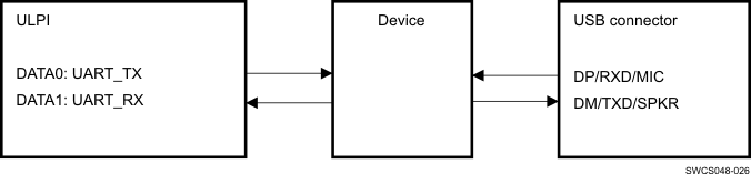 Figure 5-15 USB UART Data Flow
The OTG block integrates three main functions:
- The USB plug detection function on VBUS and ID
- The ID resistor detection
- The VBUS level detection
5.6 Charger Detection
To support Battery Charging Specification v1.1 [BCS v1.1], a charger detection module is included in the TPS65921 USB module.
The detection mechanism aims distinguishing several types of power sources that can be connected on VBUS line:
- Dedicated charger port
- Standard host port
- Charging host port
The hardware includes:
- A dedicated voltage referenced pullup on DP line
- A dedicated current controlled pulldown on DM line
- A detection comparator on DM line
- A control/detection state-machine including timers
Additional circuitry is added on DP/DM respectively for data line symmetry (required for HS operation) and for possible future extension
ID pin status detection (as defined per OTG v1.3 standard) and DP/DM single-ended receivers (as defined per USB v2.0 standard) are also used to determine the type of device plugged on the USB connector.
For details on the detection mechanism, refer to [BCS v1.1] (1).
The charging detection feature has two modes (description of each mode follows):
- Software CTL mode: Software has direct control of current source and USB charger detection comparator on DP/DM (enabled when USB_SW_CTRL_EN=1) using USB_CHRG_CTRL registers bits.
- Software FSM mode: Software can start and stop USB charger detection state-machine.
For both modes, DPPULLDOWN and DMPULLDOWN bits in OTG_CTRL register are 1 by default. This can cause errors in charger detection. Therefore, both bits must be cleared to 0 before software begins charger detection sequence.
1- Software CTL Mode (Manual detection):
When in this mode the charger detection circuitry is fully under control of software. Refer to POWER_CONTROL register bits as to how to control the detection circuitry.
Conditions:
- The TPS65921 device is powered and is in active mode.
- USB_SW_CHRG_CTRL_EN = 1, register bit set by the software
- USB_CHG_DET_EN_SW = 1, register bit set by the software
Control the USB_SW_CHRF_CTRL register to achieve charger detection.
2- Software FSM Mode (Automatic detection):
The TPS65921 also supports automated battery charger detection through the USB battery charger detection FSM in Figure 5-16 while the chip is in active mode. This mode is set by software using the SW_USB_DET bit. When in this mode, the automated charger detection finite state-machine (FSM) is enabled. Refer to the state-machine diagram for details.
Conditions:
- The TPS65921 device is powered and is in active mode.
- USB_HW_CHRG_DET_EN = 1
See the Register Map for more details.
The TPS65921 device also supports automated data contact detection in the FSM through the DATA_CONTACT_DET_EN bit which should be set at the same time as SW_USB_DET above, before setting SW_CONTROL bit. This enables a block of the FSM, which performs data contact detect for a maximum of DCD_TIMEOUT before automatically skipping to charger detection.
See Figure 5-16,USB Battery Charger FSM, for details of how context is stored if SW_CONTROL bit is set while in software FSM mode.
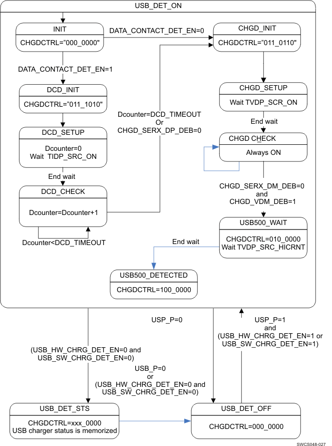 Figure 5-16 USB Battery Charger Detection FSM
USB charger detection status bit definition:
- USBVBUS_PRES: Detect presence of valid VBUS. Comparator output is debounced for DEBVBUS_TIME (minimum 10 ms) on CKCHG and generates a USB_P signal. USB_P is computed only if a battery presence is detected.
- USBCHRG_PRES: Detect presence of USB charger on DP/DM. The feature is enabled through the USB_DET_EN signal, then USBPHY performs checks on DP/DM and return status USB_DET_RESULT:
- 1 : USB 500-mA charger is detected.
- 0 : USB 100-mA charger is detected.
- USB_DET_STATUS: 500-mA/100-mA USB charger detect presence comparator output is debounced during DEBUSBCHG_TIME (minimum 20 ms) on CKCHG, debounced signal is USB_DET_RESULT (set to 1 in case of 500-mA charger)
- Two signals are the result of the charger detection state machine:
- USB100_P: Valid 100-mA charger (VBUS supplier) is detected.
- USB500_P: Valid 500-mA charger (USB charger) is detected.
5.6.1 USB Battery Charger FSM
The FSM uses the control signals CHGDCTRL[6:0] described below to control and observe battery charger detection.
When the SW_CONTROL bit is set to 1, the current context of the FSM and the state of charger detection is latched in POWER_CONTROL register bits HWDETECT, DP_VSRC_EN, VDAT_DET, and DET_COMP, after which FSM control signals CHGDCTRL[6:0] are ignored, and charger detection hardware and the CHGR_DET pin are controlled by the software.
The CHGD_IDP_SRC_EN bit is not latched when the SW_CONTROL bit is set (for example, if the FSM is performing data-contact detection at the time the SW_CONTROL is set to 1, the CHGD_IDP_SRC_EN bit is unchanged — its default value is 0).
5.6.2 FSM Control Signals
Table 5-1 USB Charger Detect FSM I/O Control Signals
| CONTROL SIGNAL | CONTROL SIGNAL | DESCRIPTION | TYPE |
|---|---|---|---|
| Bit(6) | USB500_P | 500-mA USB charging can be enabled | Input |
| Bit(5) | USB100_P | 100-mA USB charging can be enabled | Input |
| Bit(4) | CHGD_DET_EN | Enable charger detection (used to enable CHGD IBIAS block) | Output |
| Bit(3) | CHGD_IDP_SRC_EN | Enable IDP_SRC and RDM_DWN | Output |
| Bit(2) | CHGD_VDP_SRC_EN | Enable VDP_SRC buffer, IDM_SINK, and VDAT_REF_DM comp | Output |
| Bit(1) | CHGD_SERX_EN | Enable SERX comparators on DP and DM | Output |
| Bit(0) | Reserved | Reserved | Output |
Table 5-1 shows control signals used to control the charger detection analog block from the FSM. The bit number in the left-handed column indicates control bit position used in the charger detection state-machine. Both SERX comparator outputs (CHGD_SERX_DP, CHGD_SERX_DM) are available for register read in the VENDOR_SPECIFIC3 register.
Example:
State: DCD_INIT
Control: CHGDCTRL[6:0] = 011_1010
Bit(6): USB500_P = 0
Bit(5): USB100_P = 1
Bit(4): CHGD_DET_EN = 1
Bit(3): CHGD_IDP_SRC_EN = 1
Bit(2): CHGD_VDP_SRC_EN = 0
Bit(1): CHGD_SERX_EN = 1
Bit(0): Reserved = 0
5.7 MADC
The Monitoring Analog-to-Digital Convertor (MADC) enables the host processors to monitor analog signals using Analog-to-Digital Conversion (ADC). After the conversion is complete, the host processor reads the results of the conversion through the inter-integrated circuit (I2C) interface.
The MADC has the following features:
- 10-bit ADC
- External input (ADCIN0)
- Internal inputs (VBUS and battery voltage)
- MADC resource shared among multiple users, including system host processors and the internal USB
- Four ways of starting analog-to-digital (ADC) conversion
- Quarter-bit accuracy if the averaging function is used for modem-initiated real-time (RT) conversion requests
- Management of potential concurrent conversion requests and priority between different resource users
- Interrupt signal to the primary interrupt handler (PIH) module at the end-of-sequence of conversions
- Averaging feature to sample the input channel on four consecutive conversion cycles instead of once, and to provide the average value of four conversions
Because the MADC is shared by users, there are four ways to start the ADC conversion. Three of these requests can be triggered by external host processors, and one request is issued by USB:
- Hardware or RT conversion request: This request is initiated by the external host processor to request RT signal conversion. This conversion request is most useful when tied to a modem processor request for battery voltage level, in synchronization with a signal frame boundary. The host processor can request conversion on all ADC input channels using this conversion request.
- SW1 software conversion request: This request can be initiated by the first external host processor to request non-RT conversions. This request is also called an asynchronous or GP conversion (GPC) request.
- SW2 software conversion request: This request can be initiated by the second external host processor to request non-RT conversions. This request is also called an asynchronous or GPC request.
- USB conversion request: This is a GPC request triggered by the USB through TPS65921 internal signals. This conversion request is for the ADCIN12 channel.
It is possible to delay the conversion by programming the acquisition time (ACQUISITION register).
5.8 JTAG Interfaces
The TPS65921 JTAG TAP controller handles standard IEEE JTAG interfaces. This section describes the timing requirements for the tools used to test the TPS65921 power management.
The JTAG/TAP module provides a JTAG interface according to IEEE Std1149.1a. This interface uses the four I/O pins TMS, TCK, TDI, and TDO. The TMS, TCK, and TDI inputs contain a pullup device, which makes their state high when they are not driven. The output TDO is a 3-state output, which is high impedance except when data are shifted between TDI and TDO.
- TCK is the test clock signal.
- TMS is the test mode select signal.
- TDI is the scan path input.
- TDO is the scan path output.
TMS and TDO are multiplexed at the top level with the CPIO0 and CPIO1 pins. The dedicated external TEST pin switches from functional mode (GPIO0/GPIO1) to JTAG mode (TMS/TDO). The JTAG operations are controlled by a state-machine that follows the IEEE Std1149.1a state diagram. This state-machine is reset by the TPS65921 internal power-on reset. A test mode is selected by writing a 6-bit word (instruction) into the instruction register and then accessing the related data register.
5.8.1 Keyboard
The keyboard is connected to the chip using:
- KBR (7:0) input pins for row lines
- KBC (7:0) output pins for column lines
Figure 5-17 shows the keyboard connection.
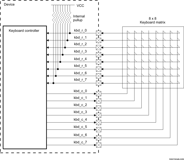 Figure 5-17 Keyboard Connection
When a key button of the keyboard matrix is pressed, the corresponding row and column lines are shorted together. To allow key press detection, all input pins (KBR) are pulled up to VCC and all output pins (KBC) driven to a low level.
Any action on a button generates an interrupt to the sequencer.
The decoding sequence is written to allow detection of simultaneous press actions on several key buttons.
The keyboard interface can be used with a smaller keyboard area than 8 × 8. To use a 6 × 6 keyboard, KBR(6) and KBR(7) must be tied high to prevent any scanning process distribution.