JAJS386I April   2004  – November 2023 TPS715A

PRODUCTION DATA  

  1.   1
  2. 特長
  3. アプリケーション
  4. 概要
  5. Pin Configuration and Functions
  6. Specifications
    1. 5.1 Absolute Maximum Ratings
    2. 5.2 ESD Ratings
    3. 5.3 Recommended Operating Conditions
    4. 5.4 Thermal Information
    5. 5.5 Electrical Characteristics
    6. 5.6 Typical Characteristics
  7. Detailed Description
    1. 6.1 Overview
    2. 6.2 Functional Block Diagrams
    3. 6.3 Feature Description
      1. 6.3.1 Wide Supply Range
      2. 6.3.2 Low Supply Current
      3. 6.3.3 Current Limit
      4. 6.3.4 Dropout Voltage (VDO)
    4. 6.4 Device Functional Modes
      1. 6.4.1 Normal Operation
      2. 6.4.2 Dropout Operation
  8. Application and Implementation
    1. 7.1 Application Information
    2. 7.2 Typical Applications
      1. 7.2.1 Design Requirements
      2. 7.2.2 Detailed Design Procedure
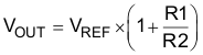
        1. 7.2.2.1 Setting VOUT for the TPS715A01 Adjustable LDO
        2. 7.2.2.2 External Capacitor Requirements
        3. 7.2.2.3 Input and Output Capacitor Requirements
        4. 7.2.2.4 Reverse Current
        5. 7.2.2.5 Feed-Forward Capacitor (CFF)
        6. 7.2.2.6 Power Dissipation (PD)
        7. 7.2.2.7 Estimating Junction Temperature
      3. 7.2.3 Application Curves
    3. 7.3 Best Design Practices
    4. 7.4 Power Supply Recommendations
    5. 7.5 Layout
      1. 7.5.1 Layout Guidelines
        1. 7.5.1.1 Power Dissipation
      2. 7.5.2 Layout Example
  9. Device and Documentation Support
    1. 8.1 Device Support
      1. 8.1.1 Development Support
        1. 8.1.1.1 Evaluation Module
        2. 8.1.1.2 Spice Models
      2. 8.1.2 Device Nomenclature
    2. 8.2 Documentation Support
      1. 8.2.1 Related Documentation
    3. 8.3 ドキュメントの更新通知を受け取る方法
    4. 8.4 サポート・リソース
    5. 8.5 Trademarks
    6. 8.6 静電気放電に関する注意事項
    7. 8.7 用語集
  10. Revision History
  11. 10Mechanical, Packaging, and Orderable Information

パッケージ・オプション

メカニカル・データ(パッケージ|ピン)
サーマルパッド・メカニカル・データ
発注情報

Setting VOUT for the TPS715A01 Adjustable LDO

The TPS715A contains an adjustable version, the TPS715A01, which sets the output voltage using an external resistor divider as shown in Figure 7-2. The output voltage operating range is 1.205 V to 15 V, and is calculated using:

Equation 2. GUID-D25991CD-372F-448E-B05A-77219B3D168A-low.gif

where:

  • VREF = 1.205 V (typical)

Choosing resistors R1 and R2 allows approximately 1.5 μA of current through the resistor divider. Lower value resistors can be used for improved noise performance, but consume more power. Avoid higher resistor values because leakage current into or out of FB across R1 / R2 creates an offset voltage that is proportional to VOUT divided by VREF. The recommended design procedure is to choose R2 = 1 MΩ to set the divider current at 1.5 μA, and then calculate R1 using Equation 3:

Equation 3. R1 = VOUTVREF - 1×R2

Figure 7-2 depicts this configuration.