SBVS191B April 2012 – August 2014
PRODUCTION DATA.
- 1 Features
- 2 Applications
- 3 Description
- 4 Revision History
- 5 Pin Configuration and Functions
- 6 Specifications
- 7 Detailed Description
- 8 Application and Implementation
- 9 Power-Supply Recommendations
- 10Layout
- 11Device and Documentation Support
- 12Mechanical, Packaging, and Orderable Information
パッケージ・オプション
デバイスごとのパッケージ図は、PDF版データシートをご参照ください。
メカニカル・データ(パッケージ|ピン)
- YZY|5
サーマルパッド・メカニカル・データ
発注情報
5 Pin Configuration and Functions
YZY Package
DSBGA-5
(Top View)
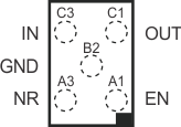
Pin Functions
| PIN | I/O | DESCRIPTION | |
|---|---|---|---|
| NAME | NO. | ||
| EN | A1 | I | Driving this pin high turns on the regulator. Driving this pin low puts the regulator into shutdown mode. EN can be connected to IN if not used. |
| GND | B2 | — | Ground |
| IN | C3 | I | Input supply |
| NR | A3 | — | Noise reduction; connecting this pin to an external capacitor bypasses noise generated by the internal band gap. This capacitor allows output noise to be reduced to very low levels. |
| OUT | C1 | O | Output of the regulator. To assure stability, a small ceramic capacitor (total typical capacitance ≥ 2.0 μF) is required from this pin to ground. |