JAJSEQ7D February   2018  – August 2019 TPS7A05

PRODUCTION DATA.  

  1. 特長
  2. アプリケーション
  3. 概要
    1.     Device Images
      1.      代表的なアプリケーション回路
      2.      グランド電流と出力電流との関係
  4. 改訂履歴
  5. Pin Configuration and Functions
    1.     Pin Functions
  6. Specifications
    1. 6.1 Absolute Maximum Ratings
    2. 6.2 ESD Ratings
    3. 6.3 Recommended Operating Conditions
    4. 6.4 Thermal Information
    5. 6.5 Electrical Characteristics
    6. 6.6 Switching Characteristics
    7. 6.7 Typical Characteristics
  7. Detailed Description
    1. 7.1 Overview
    2. 7.2 Functional Block Diagram
    3. 7.3 Feature Description
      1. 7.3.1 Excellent Transient Response
      2. 7.3.2 Active Discharge
      3. 7.3.3 Low IQ in Dropout
      4. 7.3.4 Undervoltage Lockout (UVLO)
      5. 7.3.5 Enable
      6. 7.3.6 Internal Foldback Current Limit
      7. 7.3.7 Thermal Shutdown
    4. 7.4 Device Functional Modes
      1. 7.4.1 Normal Mode
      2. 7.4.2 Dropout Mode
      3. 7.4.3 Disable Mode
  8. Application and Implementation
    1. 8.1 Application Information
      1. 8.1.1 Recommended Capacitor Types
      2. 8.1.2 Input and Output Capacitor Requirements
      3. 8.1.3 Special Considerations When Ramping Down VIN and Enable
      4. 8.1.4 Load Transient Response
      5. 8.1.5 Dropout Voltage
        1. 8.1.5.1 Behavior When Transitioning From Dropout Into Regulation
        2. 8.1.5.2 Behavior of Output Resulting From Line Transient When in Dropout
      6. 8.1.6 Undervoltage Lockout (UVLO) Operation
      7. 8.1.7 Power Dissipation (PD)
        1. 8.1.7.1 Estimating Junction Temperature
        2. 8.1.7.2 Recommended Area for Continuous Operation
    2. 8.2 Typical Application
      1. 8.2.1 Design Requirements
      2. 8.2.2 Design Considerations
      3. 8.2.3 Application Curve
  9. Power Supply Recommendations
  10. 10Layout
    1. 10.1 Layout Guidelines
    2. 10.2 Layout Example
  11. 11デバイスおよびドキュメントのサポート
    1. 11.1 デバイス・サポート
      1. 11.1.1 SPICEモデル
      2. 11.1.2 デバイスの項目表記
    2. 11.2 ドキュメントのサポート
      1. 11.2.1 関連資料
    3. 11.3 ドキュメントの更新通知を受け取る方法
    4. 11.4 コミュニティ・リソース
    5. 11.5 商標
    6. 11.6 静電気放電に関する注意事項
    7. 11.7 Glossary
  12. 12メカニカル、パッケージ、および注文情報

パッケージ・オプション

メカニカル・データ(パッケージ|ピン)
サーマルパッド・メカニカル・データ
発注情報

Undervoltage Lockout (UVLO) Operation

The UVLO circuit ensures that the device stays disabled before its input supply reaches the minimum operational voltage range, and ensures that the device shuts down when the input supply collapses. See Figure 46 for rising and falling thresholds. Figure 51 depicts the UVLO circuit response to various input voltage events. The diagram can be separated into the following parts:

  • Region A: The device does not start until the input reaches the UVLO rising threshold
  • Region B: Normal operation, regulating device
  • Region C: Brownout event above the UVLO falling threshold (UVLO rising threshold – UVLO hystersis). The output may fall out of regulation but the device is still enabled.
  • Region D: Normal operation, regulating device
  • Region E: Brownout event below the UVLO falling threshold. The device is disabled in most cases and the output falls as a result of the load and active discharge circuit. The device is re-enabled when the UVLO rising threshold is reached by the input voltage and a normal start-up follows.
  • Region F: Normal operation followed by the input falling to the UVLO falling threshold
  • Region G: The device is disabled as the input voltage falls below the UVLO falling threshold to 0 V. The output falls as a result of the load and active discharge circuit.
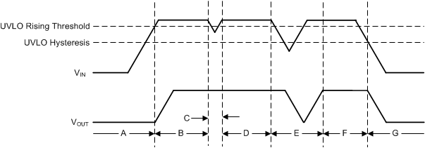
TPS7A05 ai_UVLO_Operation_SBVS267.gifFigure 51. Typical UVLO Operation