at TJ = 25°C, VIN =
VOUT(TARGET) + 0.3 V, IOUT = 25 mA, V(EN) =
VIN, CIN = 10 μF, COUT = 10 μF,
C(SS) = 10 nF, and the PG pin pulled up to VIN with a
100-kΩ pullup resistor (unless otherwise noted)
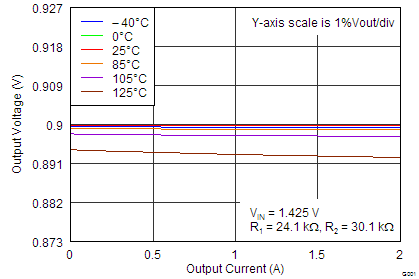
 Figure 5-1 Load
Regulation (0.9 V, Adjustable)
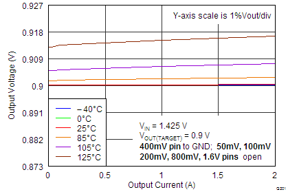
 Figure 5-3 Load
Regulation (0.9 V, Fixed By Setting Pins)
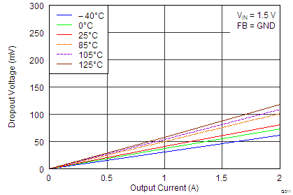
 Figure 5-5 Dropout Voltage vs Output Current
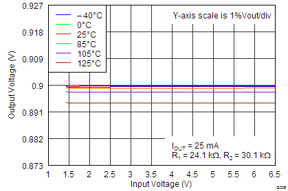
 Figure 5-7 Line
Regulation (0.9 V, Adjustable)
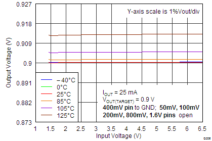
 Figure 5-9 Line
Regulation (0.9 V, Fixed By Setting Pins)
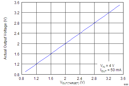
 Figure 5-11 Measured Output Voltage vs Pin Setting
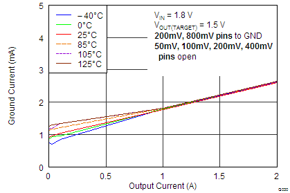
 Figure 5-13 GND
Pin Current vs Output Current
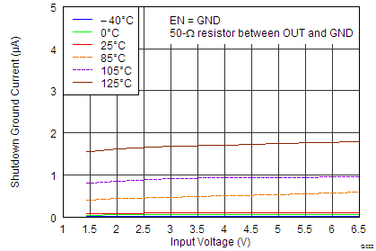
 Figure 5-15 GND
Pin Current In Shutdown vs Temperature
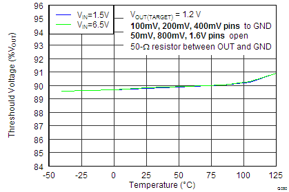
 Figure 5-17 Power-Good Threshold Voltage vs Temperature
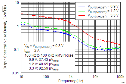
 Figure 5-19 Noise
Spectral Density By Output Voltage
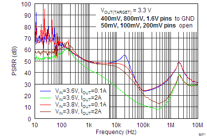
 Figure 5-21 Power-Supply Ripple Rejection vs Frequency
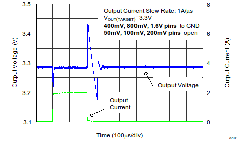
 Figure 5-23 Load
Transient Response (VOUT = 3.3 V)
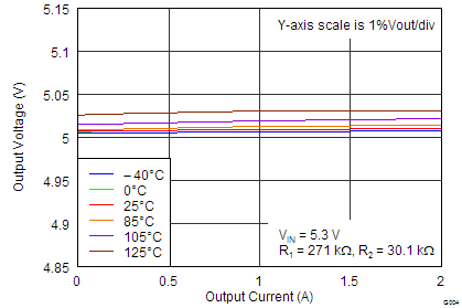
 Figure 5-2 Load
Regulation (5.0 V, Adjustable)
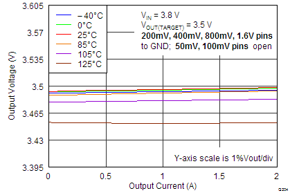
 Figure 5-4 Load
Regulation (3.5 V, Fixed By Setting Pins)
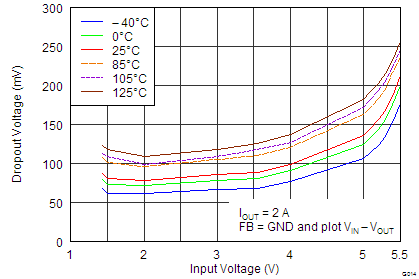
 Figure 5-6 Dropout Voltage vs Temperature
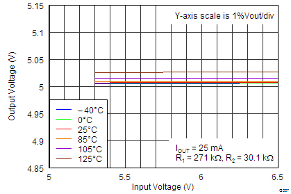
 Figure 5-8 Line
Regulation (5 V, Adjustable)
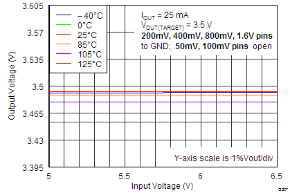
 Figure 5-10 Line
Regulation (3.5 V, Fixed By Setting Pins)
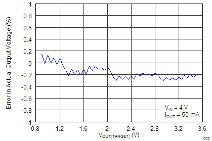
 Figure 5-12 Accuracy vs Pin Setting
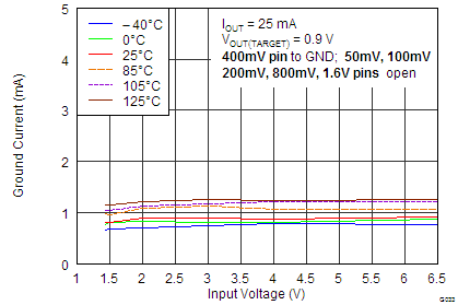
 Figure 5-14 GND
Pin Current vs Input Voltage
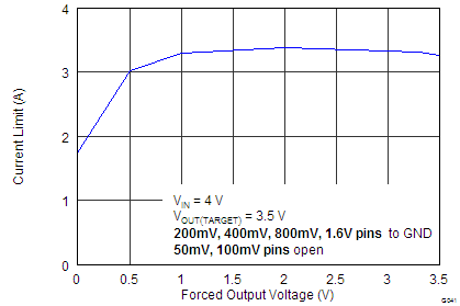
 Figure 5-16 Current Limit vs Output Voltage (Foldback)
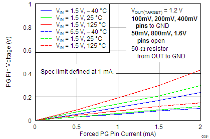
 Figure 5-18 Power-Good Pin Drive Capability
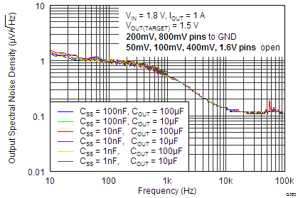
 Figure 5-20 Noise
Spectral Density By External Capacitors
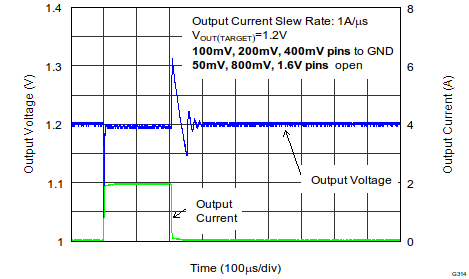
 Figure 5-22 Load
Transient Response (VOUT = 1.2 V)