JAJSC96C October 2013 – September 2016 TPS7B4250-Q1
PRODUCTION DATA.
- 1 特長
- 2 アプリケーション
- 3 概要
- 4 改訂履歴
- 5 Pin Configuration and Functions
- 6 Specifications
- 7 Detailed Description
- 8 Application and Implementation
- 9 Power Supply Recommendations
- 10Layout
- 11デバイスおよびドキュメントのサポート
- 12メカニカル、パッケージ、および注文情報
8 Application and Implementation
NOTE
Information in the following applications sections is not part of the TI component specification, and TI does not warrant its accuracy or completeness. TI’s customers are responsible for determining suitability of components for their purposes. Customers should validate and test their design implementation to confirm system functionality.
8.1 Application Information
Based on the end-application, different values of external components can be used. An application can require a larger output capacitor during fast load steps to prevent a reset from occurring. TI recommends a low ESR ceramic capacitor with a dielectric of type X5R or X7R for better load transient response.
8.2 Typical Application
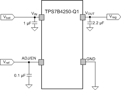
Figure 16 show typical application circuit for the TPS7B4250-Q1 device.
 Figure 16. Typical Application Schematic
8.2.1 Design Requirements
For this design example, use the parameters listed in Table 1.
Table 1. Design Parameters
| DESIGN PARAMETER | EXAMPLE VALUES |
|---|---|
| Input voltage | 4 to 40 V |
| ADJ reference voltage | 1.5 to 18 V |
| Output voltage | 1.5 to 18 V |
| Output current rating | 50 mA |
| Output capacitor range | 1 µF to 50 µF |
| Output capacitor ESR range | 1 mΩ to 20 Ω |
8.2.2 Detailed Design Procedure
To begin the design process, determine the following:
- Input voltage range
- Reference voltage
- Output voltage
- Output current rating
- Input capacitor
- Output capacitor
8.2.2.1 External Capacitors
An input capacitor, CI, is recommended to buffer line influences. Connect the capacitors close to the IC pins.
The output capacitor for the TPS7B4250-Q1 device is required for stability. Without the output capacitor, the regulator oscillates. The actual size and type of the output capacitor can vary based on the application load and temperature range. The effective series resistance (ESR) of the capacitor is also a factor in the IC stability. The worst case is determined at the minimum ambient temperature and maximum load expected. To ensure stability of TPS7B4250-Q1 device, the device requires an output capacitor between 1 µF and 50 µF with an ESR range between 0.001 Ω and 20 Ω that can cover most types of capacitor ESR variation under the recommend operating conditions. As a result, the output capacitor selection is flexible.
The capacitor must also be rated at all ambient temperature expected in the system. To maintain regulator stability down to –40°C, use a capacitor rated at that temperature.
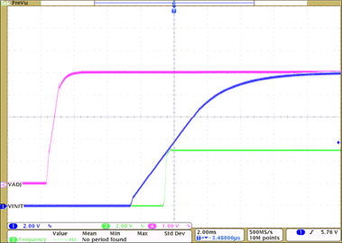
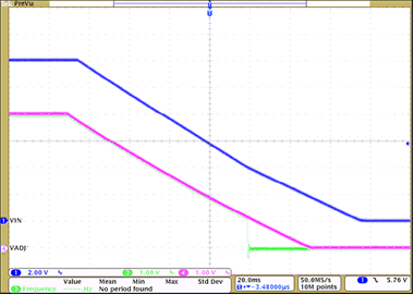
8.2.3 Application Curves

| VI = 12 V | VADJ = 5 V | |

| VI = 12 V | VADJ = 5 V | |