SLVSCD1C December 2013 – November 2015 TPS92561
PRODUCTION DATA.
- 1 Features
- 2 Applications
- 3 Description
- 4 Revision History
- 5 Pin Configuration and Functions
- 6 Specifications
- 7 Detailed Description
-
8 Application and Implementation
- 8.1 Application Information
- 8.2
Typical Applications
- 8.2.1 Offline Boost Schematic for Design Example
- 8.2.2 11-W, 120-VAC Input, 225-V Output, Offline Boost Design Example
- 9 Power Supply Recommendations
- 10Layout
- 11Device and Documentation Support
- 12Mechanical, Packaging, and Orderable Information
パッケージ・オプション
メカニカル・データ(パッケージ|ピン)
- DGN|8
サーマルパッド・メカニカル・データ
- DGN|8
発注情報
6 Specifications
6.1 Absolute Maximum Ratings
over operating free-air temperature range (unless otherwise noted) (1)| MIN | MAX | UNIT | ||
|---|---|---|---|---|
| Pin voltage range(2) | SRC, SEN, ADJ, OVP | –0.3 | 5 | V |
| VP | –1 | 45 | ||
| VCC | –0.3 | 12 | ||
| Tstg | Storage temperature | –60 | 150 | °C |
| TJ | Junction temperature | Internally Limited | ||
(1) Stresses beyond those listed under "absolute maximum ratings” may cause permanent damage to the device. These are stress ratings only and functional operation of the device at these or any other conditions beyond those indicated under “recommended operating conditions” is not implied. Exposure to absolute-maximum-rated conditions for extended periods may affect device reliability.
(2) All voltages are with respect to network ground terminal.
6.2 ESD Ratings
| VALUE | UNIT | |||
|---|---|---|---|---|
| V(ESD) | Electrostatic discharge | Human-body model (HBM), per ANSI/ESDA/JEDEC JS-001(1)(3) | ±1500 | V |
| Charged-device model (CDM), per JEDEC specification JESD22-C101(2) | ±1500 | |||
(1) JEDEC document JEP155 states that 500-V HBM allows safe manufacturing with a standard ESD control process.
(2) JEDEC document JEP157 states that 250-V CDM allows safe manufacturing with a standard ESD control process.
(3) ESD testing is performed according to the respective JESD22 JEDEC standard.
6.3 Recommended Operating Conditions
over operating free-air temperature range (unless otherwise noted)| MIN | NOM | MAX | UNIT | ||
|---|---|---|---|---|---|
| VP | Supply voltage | 6.5 | 42 | V | |
| TJ | Operating junction temperature | –40 | 125 | °C | |
6.4 Thermal Information
over operating free-air temperature range (unless otherwise noted)| THERMAL METRIC(1) | TPS92561 | UNIT | |
|---|---|---|---|
| DGN (HVSSOP) | |||
| 8 PINS | |||
| RθJA | Junction-to-ambient thermal resistance | 65.3 | °C/W |
| RθJC(top) | Junction-to-case (top) thermal resistance | 64.8 | °C/W |
| RθJB | Junction-to-board thermal resistance | 44.8 | °C/W |
| ψJT | Junction-to-top characterization parameter | 3.9 | °C/W |
| ψJB | Junction-to-board characterization parameter | 44.6 | °C/W |
| RθJC(bot) | Junction-to-case (bottom) thermal resistance | 13.2 | °C/W |
(1) For more information about traditional and new thermal metrics, see the Semiconductor and IC Package Thermal Metrics application report, SPRA953.
6.5 Electrical Characteristics
over recommended operating conditions with –40°C ≤ TJ ≤ 125°C. VCC = 12 V. CVCC = 0.47 µF| PARAMETER | TEST CONDITIONS | MIN | TYP | MAX | UNIT | |
|---|---|---|---|---|---|---|
| SUPPLY | ||||||
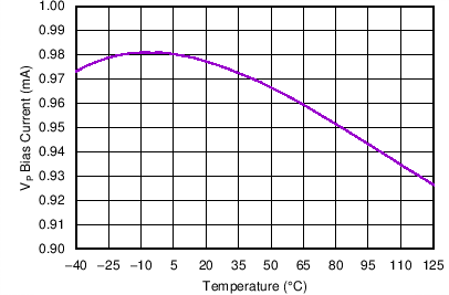
| IIN | VP operating current | 6.5 V < VVP < 42 V | 0.5 | 1 | 1.6 | mA |
| VCC REGULATOR | ||||||
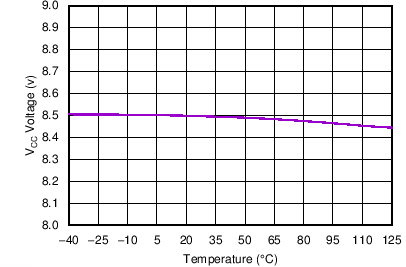
| VCC | VCC regulated voltage | ICC ≤ 10 mA CVCC = 0.47 µF 12 V < VVP < 42 V |
7.75 | 8.35 | 8.95 | V |
| ICC = 10 mA CVCC = 0.47 µF VVP = 6.5 V |
5.42 | 5.92 | 6.42 | |||
| ICC = 0 mA CVCC = 0.47 µF VVP = 2 V |
2 | |||||
| ICC-LIM | VCC current limit | VCC = 0 V 6.5 V < VVP < 42 V |
20 | 34 | 56 | mA |
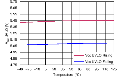
| VCC-UVLO-UPTH | VCC UVLO rising threshold | 5 | 5.44 | 5.85 | V | |
| VCC-UVLO-LOTH | VCC UVLO falling threshold | 4.68 | 5.07 | 5.46 | V | |
| MOSFET GATE DRIVER | ||||||
| VGATE-HIGH | Gate driver output high | With respect to SRC Sinking 100 mA from GATE Force VCC = 9.5 V |
8 | 8.71 | 9.41 | V |
| VGATE-LOW | Gate driver output low | With respect to SRC Sourcing 100 mA to GATE |
10 | 180 | 350 | mV |
| tRISE | VGATE rise time | CGATE = 1 nF across GATE and SRC | 37 | ns | ||
| tFALL | VGATE fall time | CGATE = 1 nF across GATE and SRC | 30 | |||
| tRISE-PG-DELAY | VGATE low-to-high propagation delay | CGATE = 1 nF across GATE and SRC | 91 | |||
| tFALL-PG-DELAY | VGATE high-to-low propagation delay | CGATE = 1 nF across GATE and SRC | 112 | |||
| CURRENT SOURCE AT ADJ PIN | ||||||
| IADJ-STARTUP | Output current of ADJ pin at start-up | VADJ < 90 mV | 14 | 20 | 26 | µA |
| CURRENT SENSE AMPLIFIER | ||||||
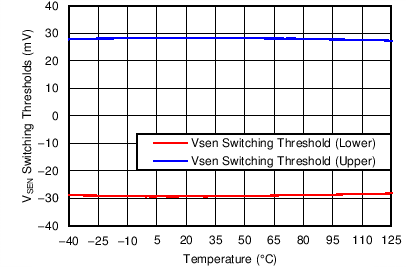
| VSEN-UPPER-TH | VSEN upper threshold over VADJ | VSEN – VADJ
VADJ = 0.2 V VGATE at falling edge |
17.6 | 29.3 | 41 | mV |
| VSEN-LOWER-TH | VSEN lower threshold over VADJ | VSEN – VADJ
VADJ = 0.2 V VGATE at rising edge |
–40.7 | –29.1 | –17.5 | |
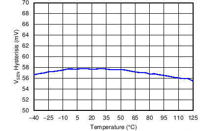
| VSEN-HYS | VSEN hysteresis | (VSEN-UPPER-TH – VSEN-LOWER-TH) | 40.9 | 60 | 75.9 | |
| VSEN-OFFSET | VSEN offset with respect to VADJ | (VSEN-UPPER-TH + VSEN-LOWER-TH) / 2 | –4 | –0.1 | 4 | |
| OUTPUT OVERVOLTAGE PROTECTION (OVP) | ||||||
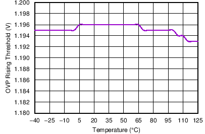
| VOVP-UPTH | Output overvoltage detection upper threshold | VOVP increasing, VGATE at falling edge | 1.11 | 1.19 | 1.27 | V |
| VOVP-HYS | Output overvoltage detection hysteresis | VOVP-UPTH – VOVP-LOTH | 15 | 44 | 80 | mV |
| THERMAL SHUTDOWN | ||||||
| TSD | Thermal shutdown temperature | TJ rising | 165 | °C | ||
| TSD-HYS | Thermal shutdown temperature hysteresis | TJ falling | 30 | |||
6.6 Typical Characteristics
VP = VP_NOM = 12 V