JAJSE85B October   2017  – January 2020 TPS92610-Q1

PRODUCTION DATA.  

  1. 特長
  2. アプリケーション
  3. 概要
    1.     代表的なアプリケーションの図
  4. 改訂履歴
  5. Pin Configuration and Functions
    1.     Pin Functions
  6. Specifications
    1. 6.1 Absolute Maximum Ratings
    2. 6.2 ESD Ratings
    3. 6.3 Recommended Operating Conditions
    4. 6.4 Thermal Information
    5. 6.5 Electrical Characteristics
    6. 6.6 Timing Requirements
    7. 6.7 Typical Characteristics
  7. Detailed Description
    1. 7.1 Overview
    2. 7.2 Functional Block Diagram
    3. 7.3 Feature Description
      1. 7.3.1 Device Bias
        1. 7.3.1.1 Power-On Reset (POR)
        2. 7.3.1.2 Low-Quiescent-Current Fault Mode
      2. 7.3.2 Constant-Current Driver
      3. 7.3.3 Device Enable
      4. 7.3.4 PWM Dimming
      5. 7.3.5 Diagnostics
        1. 7.3.5.1 DIAGEN
        2. 7.3.5.2 Low-Dropout Mode
        3. 7.3.5.3 Open-Circuit Detection
        4. 7.3.5.4 Short-to-GND Detection
        5. 7.3.5.5 Single-LED-Short Detection
        6. 7.3.5.6 Overtemperature Protection
      6. 7.3.6 FAULT Bus Output With One-Fails–All-Fail
    4. 7.4 Device Functional Modes
      1. 7.4.1 Undervoltage Lockout, V(SUPPLY)<V(POR_rising)
      2. 7.4.2 Normal Operation V(SUPPLY) ≥ 4.5 V
      3. 7.4.3 Low-Voltage Dropout
      4. 7.4.4 Fault Mode
  8. Application and Implementation
    1. 8.1 Application Information
    2. 8.2 Typical Application
      1. 8.2.1 Single-Channel LED Driver With Full Diagnostics
        1. 8.2.1.1 Design Requirements
        2. 8.2.1.2 Detailed Design Procedure
        3. 8.2.1.3 Application Curve
      2. 8.2.2 Single-Channel LED Driver With Heat Sharing
        1. 8.2.2.1 Design Requirements
        2. 8.2.2.2 Detailed Design Procedure
        3. 8.2.2.3 Application Curve
  9. Layout
    1. 9.1 Layout Guidelines
    2. 9.2 Layout Example
  10. 10デバイスおよびドキュメントのサポート
    1. 10.1 ドキュメントのサポート
      1. 10.1.1 関連資料
    2. 10.2 ドキュメントの更新通知を受け取る方法
    3. 10.3 コミュニティ・リソース
    4. 10.4 商標
    5. 10.5 静電気放電に関する注意事項
    6. 10.6 Glossary
  11. 11メカニカル、パッケージ、および注文情報

パッケージ・オプション

メカニカル・データ(パッケージ|ピン)
サーマルパッド・メカニカル・データ
発注情報

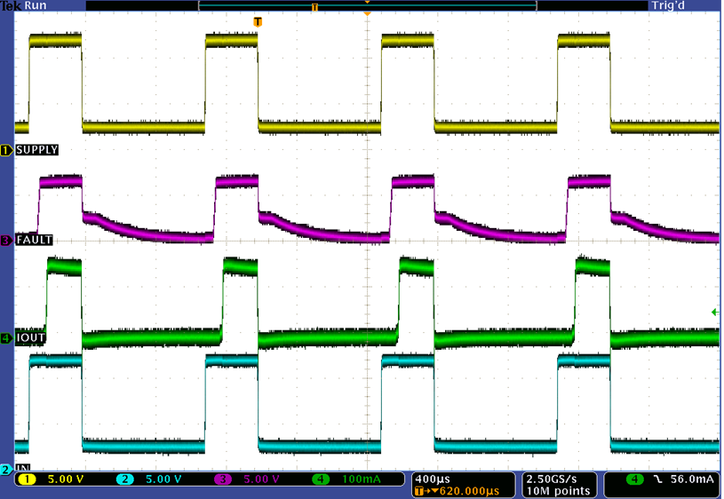
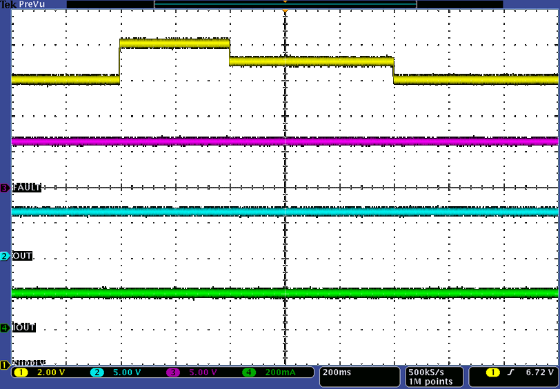
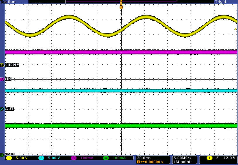
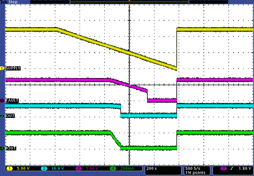
Typical Characteristics

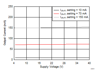
TPS92610-Q1 D001-IOUT-SUPPLY-SLDS233.gif
Figure 2. Output Current vs Supply Voltage
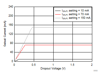
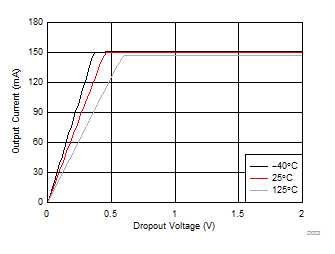
TPS92610-Q1 D002-IOUT-VDROP-SLDS233.gif
Figure 4. Output Current vs Dropout Voltage
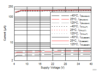
TPS92610-Q1 D004-IQ-SUPPLY-SLDS233.gif
Figure 6. Shutdown, Quiescent, and Fault Current vs Supply Voltage
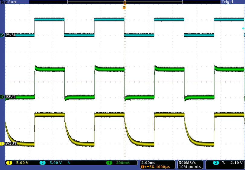
TPS92610-Q1 typ-app-pwm-dimming-external-input-slds233.png
Ch. 1 = V(OUT) Ch. 2 = V(PWM) Ch. 4 = I(OUT)
ƒ(PWM) = 200 Hz Duty cycle = 50%
Figure 8. PWM Dimming via External Input
TPS92610-Q1 sys-transient-undervoltage-slds233.png
Ch. 1 = SUPPLY Ch. 2 = V(OUT) Ch. 3 = FAULT
Ch. 4 = I(OUT)
Figure 10. Transient Undervoltage
TPS92610-Q1 sys-jump-start-slds233.png
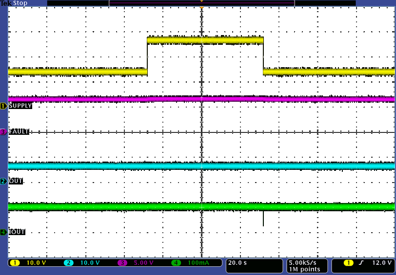
Ch. 1 = SUPPLY Ch. 2 = V(OUT) Ch. 3 = FAULT
Ch. 4 = I(OUT)
Figure 12. Jump Start
TPS92610-Q1 sys-superimposed-alternating-voltage-1k-slds233.png
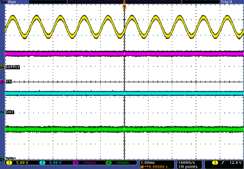
Ch. 1 = SUPPLY Ch. 2 = V(OUT) Ch. 3 = FAULT
Ch. 4 = I(OUT)
Figure 14. Superimposed Alternating Voltage, 1 kHz
TPS92610-Q1 sys-slow-decrease-and-increase-slds233.png
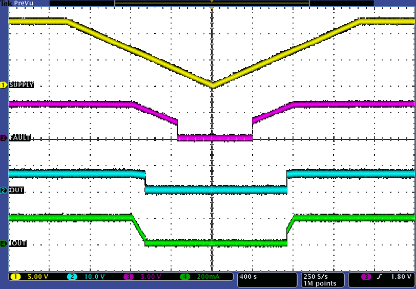
Ch. 1 = SUPPLY Ch. 2 = V(OUT) Ch. 3 = FAULT
Ch. 4 = I(OUT)
Figure 16. Slow Decrease and Slow Increase of Supply Voltage
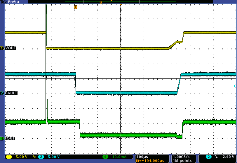
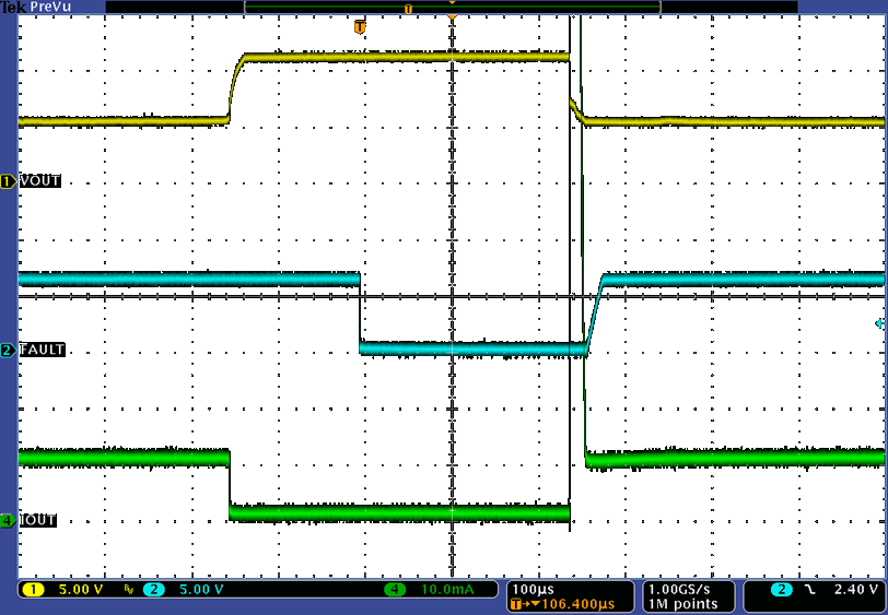
TPS92610-Q1 typ-app-led-short-circuit-slds233.png
Ch. 1 = V(OUT) Ch. 2 = FAULT Ch. 4 = I(OUT)
Figure 18. LED Short-Circuit Protection and Recovery
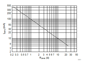
TPS92610-Q1 D001-IOUT-RES.gif
Figure 3. Output Current vs Current-Sense Resistor
TPS92610-Q1 D003-VDROP-TEMP-SLDS233.gif
Figure 5. Output Current vs Temperature
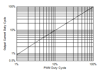
TPS92610-Q1 D005-PWMIN-OUT-SLDS233.gif
Figure 7. PWM Output Duty Cycle vs Input Duty Cycle
TPS92610-Q1 typ-app-pwm-dimming-bcm-input-slds233.png
Ch. 1 = V(SUPPLY) Ch. 2 = V(OUT) Ch. 3 = FAULT
Ch. 4 = I(OUT) f(PWM) = 1000 Hz Duty cycle = 30%
SUPPLY dimming between 2.5 V and 12 V FAULT floating
Figure 9. PWM Dimming via Power Supply
TPS92610-Q1 sys-transient-overvoltage-slds233.png
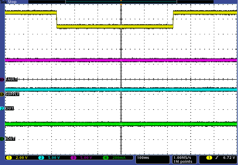
Ch. 1 = SUPPLY Ch. 2 = V(OUT) Ch. 3 = FAULT
Ch. 4 = I(OUT)
Figure 11. Transient Overvoltage
TPS92610-Q1 sys-superimposed-alternating-voltage-slds233.png
Ch. 1 = SUPPLY Ch. 2 = V(OUT) Ch. 3 = FAULT
Ch. 4 = I(OUT)
Figure 13. Superimposed Alternating Voltage, 15 Hz
TPS92610-Q1 sys-slow-decrease-quick-increase-slds233.png
Ch. 1 = SUPPLY Ch. 2 = V(OUT) Ch. 3 = FAULT
Ch. 4 = I(OUT)
Figure 15. Slow Decrease, Quick Increase of Supply Voltage
TPS92610-Q1 typ-app-led-open-circuit-slds233.png
Ch. 1 = V(OUT) Ch. 2 = FAULT Ch. 4 = I(OUT)
Figure 17. LED Open-Circuit Protection and Recovery
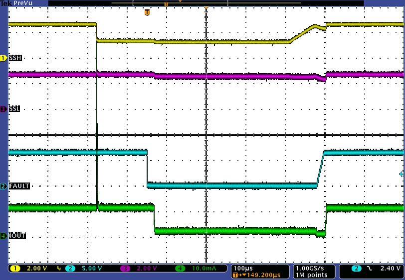
TPS92610-Q1 typ-app-single-led-short-slds233.png
Ch. 1 = V(SSH) Ch. 2 = FAULT Ch. 3 = V(SSL)
Ch. 4 = I(OUT)
Figure 19. Single-LED-Short Protection and Recovery