JAJSDC9A July   2017  – August 2017 TPSM84203 , TPSM84205 , TPSM84212

PRODUCTION DATA.  

  1. 特長
  2. アプリケーション
  3. 概要
  4. 改訂履歴
  5. Pin Configuration and Functions
  6. Specifications
    1. 6.1 Absolute Maximum Ratings
    2. 6.2 Recommended Operating Conditions
    3. 6.3 ESD Ratings
    4. 6.4 Thermal Information
    5. 6.5 Electrical Characteristics
    6. 6.6 Switching Characteristics
    7. 6.7 Typical Characteristics (VOUT = 3.3 V)
    8. 6.8 Typical Characteristics (VOUT = 5 V)
    9. 6.9 Typical Characteristics (VOUT = 12 V)
  7. Detailed Description
    1. 7.1 Overview
    2. 7.2 Functional Block Diagram
    3. 7.3 Feature Description
      1. 7.3.1 Input Capacitors
      2. 7.3.2 Output Capacitors
      3. 7.3.3 Drop-Out Voltage
      4. 7.3.4 Internal Soft-Start
      5. 7.3.5 Safe Startup into Pre-Biased Outputs
      6. 7.3.6 Over-Current Protection
      7. 7.3.7 Output Over-Voltage Protection
      8. 7.3.8 Thermal Shutdown
    4. 7.4 Device Functional Modes
      1. 7.4.1 Normal Operation
      2. 7.4.2 Eco-mode Operation
  8. Application and Implementation
    1. 8.1 Application Information
    2. 8.2 Typical Application
      1. 8.2.1 Design Requirements
      2. 8.2.2 Detailed Design Procedure
        1. 8.2.2.1 Custom Design With WEBENCH® Tools
        2. 8.2.2.2 Input and Output Capacitors
      3. 8.2.3 Application Curves
        1. 8.2.3.1 EMI
  9. Power Supply Recommendations
  10. 10Layout
    1. 10.1 Layout Guidelines
    2. 10.2 Layout Example
  11. 11デバイスおよびドキュメントのサポート
    1. 11.1 デバイス・サポート
      1. 11.1.1 開発サポート
        1. 11.1.1.1 WEBENCH®ツールによるカスタム設計
    2. 11.2 関連リンク
    3. 11.3 ドキュメントの更新通知を受け取る方法
    4. 11.4 コミュニティ・リソース
    5. 11.5 商標
    6. 11.6 静電気放電に関する注意事項
    7. 11.7 Glossary
  12. 12メカニカル、パッケージ、および注文情報

パッケージ・オプション

メカニカル・データ(パッケージ|ピン)
サーマルパッド・メカニカル・データ
発注情報

Pin Configuration and Functions

EAB Package
3-Pin Through-Hole
Top View
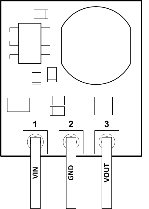
TPSM84203 TPSM84205 TPSM84212 GenPinout2.gif

Pin Functions

PIN I/O DESCRIPTION
NAME NO.
GND 2 Ground. This is the return current path for the power stage of the device. Connect this pin to the bypass capacitors associated with VIN and VOUT.
VIN 1 I Input Voltage. This pin supplies voltage to the control circuitry and power switches of the converter. Connect external bypass capacitors between this pin and GND.
VOUT 3 O Output Voltage. This pin is connected to the internal output inductor. Connect this pin to the output load and connect external bypass capacitors between this pin and GND.