JAJSFJ4H January 2005 – May 2018 TS3A5018
PRODUCTION DATA.
- 1 特長
- 2 アプリケーション
- 3 概要
- 4 改訂履歴
- 5 Pin Configuration and Functions
-
6 Specifications
- 6.1 Absolute Maximum Ratings
- 6.2 ESD Ratings
- 6.3 Recommended Operating Conditions
- 6.4 Thermal Information
- 6.5 Electrical Characteristics for 3.3-V Supply
- 6.6 Electrical Characteristics for 2.5-V Supply
- 6.7 Electrical Characteristics for 2.1-V Supply
- 6.8 Electrical Characteristics for 1.8-V Supply
- 6.9 Switching Characteristics for 3.3-V Supply
- 6.10 Switching Characteristics for 2.5-V Supply
- 6.11 Switching Characteristics for 1.8-V Supply
- 6.12 Typical Characteristics
- 7 Parameter Measurement Information
- 8 Detailed Description
- 9 Application and Implementation
- 10Power Supply Recommendations
- 11Layout
- 12デバイスおよびドキュメントのサポート
- 13メカニカル、パッケージ、および注文情報
パッケージ・オプション
デバイスごとのパッケージ図は、PDF版データシートをご参照ください。
メカニカル・データ(パッケージ|ピン)
- PW|16
- DBQ|16
- RGY|16
- D|16
- DGV|16
- RSV|16
サーマルパッド・メカニカル・データ
- RGY|16
発注情報
7 Parameter Measurement Information
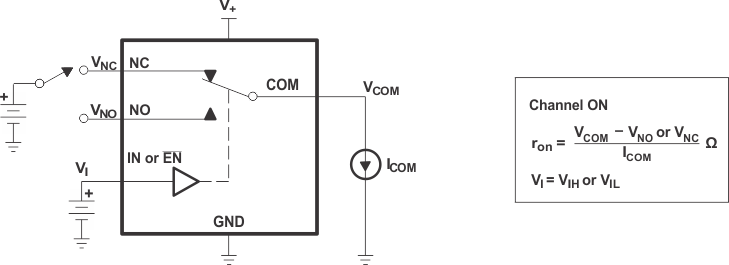 Figure 17. ON-State Resistance (ron)
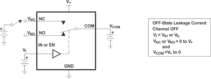 Figure 18. OFF-State Leakage Current (ICOM(OFF), INC(OFF), INO(OFF))
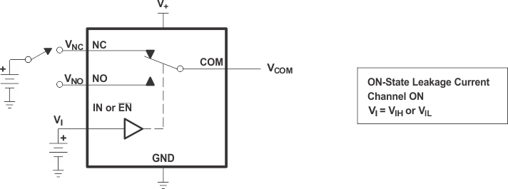 Figure 19. ON-State Leakage Current (ICOM(ON), INC(ON))
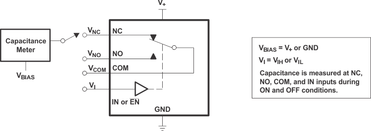 Figure 20. Capacitance (CI, CCOM(OFF), CCOM(ON), CNC(OFF), CNC(ON))
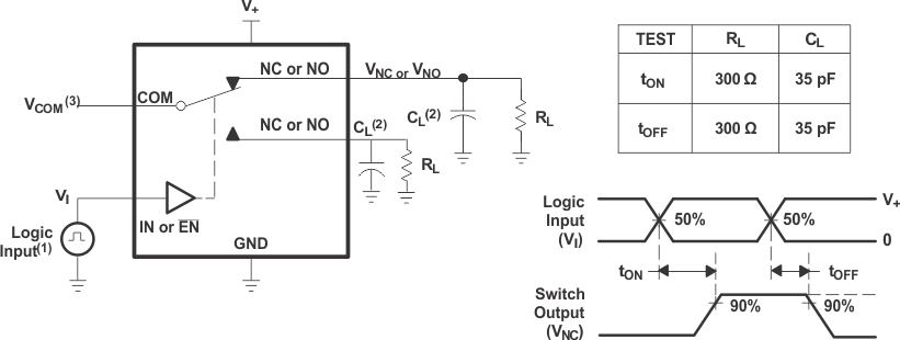
1. All input pulses are supplied by generators having the following characteristics: PRR ≤ 10 MHz, ZO = 50 Ω, tr < 5 ns, tf < 5 ns.
2. CL includes probe and jig capacitance.
3. See Electrical Characteristics for VCOM.
Figure 21. Turnon (tON) and Turnoff Time (tOFF)
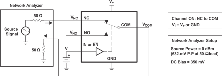 Figure 22. Bandwidth (BW)
 Figure 23. OFF Isolation (OISO)
 Figure 24. Crosstalk (XTALK)
 Figure 25. Crosstalk Adjacent

1. CL includes probe and jig capacitance.
2. All input pulses are supplied by generators having the following characteristics: PRR ≤ 10 MHz, ZO = 50 Ω, tr < 5 ns, tf < 5 ns.
Figure 26. Charge Injection (QC)
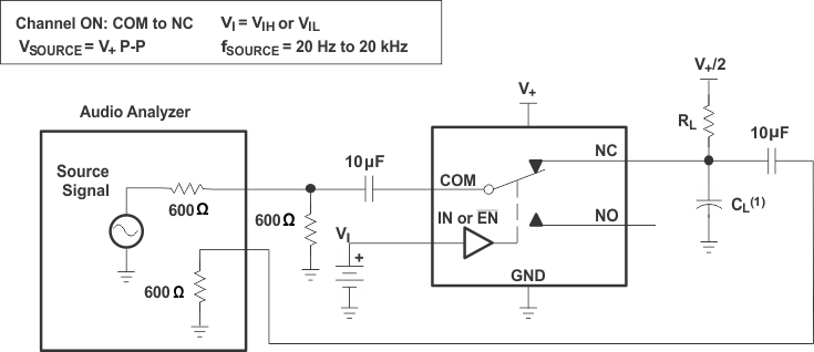
1. CL includes probe and jig capacitance.
Figure 27. Total Harmonic Distortion (THD)