SLVSC89A June 2014 – July 2014 TSC2013-Q1
PRODUCTION DATA.
- 1 Features
- 2 Applications
- 3 Description
- 4 Revision History
- 5 Pin Configurations and Functions
-
6 Specifications
- 6.1 Absolute Maximum Ratings
- 6.2 Handling Ratings
- 6.3 Recommended Operating Conditions
- 6.4 Thermal Information
- 6.5 Electrical Characteristics
- 6.6 Timing Requirements — I2C Standard Mode (ƒ(SCL) = 100 kHz)
- 6.7 Timing Requirements — I2C Fast Mode (ƒ(SCL) = 400 kHz)
- 6.8 Timing Requirements — I2C High-Speed Mode (ƒ(SCL) = 1.7 MHz)
- 6.9 Timing Requirements — I2C High-Speed Mode (ƒ(SCL) = 3.4 MHz)
- 6.10 Typical Characteristics
-
7 Detailed Description
- 7.1 Overview
- 7.2 Functional Block Diagram
- 7.3 Feature Description
- 7.4 Device Functional Modes
- 7.5 Programming
- 7.6
Register Maps
- 7.6.1 Register Content and Reset Values
- 7.6.2 Configuration and Status Registers
- 7.6.3 Data Registers
-
8 Application and Implementation
- 8.1 Application Information
- 8.2
Typical Application
- 8.2.1 Design Requirements
- 8.2.2 Detailed Design Procedure
- 8.2.3 Application Curves
- 9 Power Supply Recommendations
- 10Layout
- 11Device and Documentation Support
- 12Mechanical, Packaging, and Orderable Information
パッケージ・オプション
メカニカル・データ(パッケージ|ピン)
サーマルパッド・メカニカル・データ
発注情報
10 Layout
10.1 Layout Guidelines
The following layout suggestions should obtain optimum performance from the TSC2013-Q1 device. However, many portable applications have conflicting requirements for power, cost, size, and weight. In general, most portable devices have fairly clean power and grounds because most of the internal components are very low-power. This situation would mean less bypassing for the converter power and less concern regarding grounding. Still, each application is unique, so review the following suggestions carefully.
For optimum performance, take care with the physical layout of the TSC2013-Q1 circuitry. The basic SAR architecture is sensitive to glitches or sudden changes on the power supply, reference, and ground connections, and digital inputs that occur just prior to latching the output of the analog comparator. Therefore, during any single conversion for an n-bit SAR converter, there are n windows in which large external transient voltages can easily affect the conversion result. Such glitches might originate from switching power supplies, nearby digital logic, and high-power devices. The degree of error in the digital output depends on the reference voltage, layout, and the exact timing of the external event. The error can change if the external event changes in time with respect to the SCL input.
With this in mind, power to the TSC2013-Q1 device should be clean and well-bypassed. Add a 0.1-μF ceramic bypass capacitor between (SNSVDD and AGND) or (I/OVDD and AGND). The circuit also requires a 0.1-μF decoupling capacitor between SNSVDD/VREF and AGND. Place these capacitors as close to the device as possible. The circuit may also require a 1-μF to 10-μF capacitor if the impedance of the connection between SNSVDD/VREF and the power supply is high. Short I/OVDD to the same supply plane as SNSVDD/VREF. Short both SNSVDD/VREF and I/OVDD to the analog power-supply plane.
The ADC architecture offers no inherent rejection of noise or voltage variation in regards to using an external reference input, which is of particular concern when the reference input is tied to the power supply for auxiliary input. Any noise and ripple from the supply appears directly in the digital results. While high-frequency noise can be filtered out by the built-in MAV filter, voltage variation as a result of line frequency (50 Hz or 60 Hz) can be difficult to remove. Avoid any active trace going under the analog pins listed in the table without shielding them by a ground or power plane.
Connect the AGND pin to a clean ground point. In many cases, this connection will be the analog ground. Avoid connections that are too near the grounding point of a microcontroller or digital signal processor. If needed, run a ground trace directly from the converter to the power-supply entry or battery-connection point. The ideal layout includes an analog ground plane dedicated to the converter and associated analog circuitry.
In the specific case of use with a resistive touch screen, take care with the connection between the converter and the touch screen. Because resistive touch screens have fairly low resistance, the interconnection should be as short and robust as possible. Loose connections can be a source of error when the contact resistance changes with flexing or vibrations.
As indicated previously, noise can be a major source of error in touch-screen applications (for example, applications that require a backlit LCD panel). This electromagnetic interference (EMI) noise can coupled through the LCD panel to the touch screen and cause flickering of the converted ADC data. On can do several things to reduce this error, such as using a touch screen with a bottom-side metal layer connected to ground, which couples the majority of noise to ground. Another way to filter out this type of noise is by using the TSC2013-Q1 built-in MAV filter (see the section). Filtering capacitors, from Y+, Y–, X+, and X– to ground, can also help. Note, however, that the use of these capacitors increases screen settling time and requires longer panel voltage stabilization times, and also increases precharge and sense times for the PINTDAV circuitry of the TSC2013-Q1 device. The resistor value varies depending on the touch-screen sensor used. The internal 50-kΩ pullup resistor (R(IRQ)) may be adequate for most sensors.
10.2 Layout Example
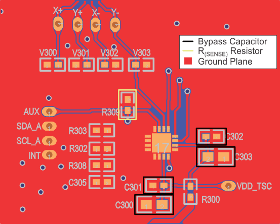 Figure 57. TSC2013-Q1 Layout Example