SCES638D October 2007 – June 2017 TXS0101
PRODUCTION DATA.
- 1 Features
- 2 Applications
- 3 Description
- 4 Revision History
- 5 Pin Configuration and Functions
-
6 Specifications
- 6.1 Absolute Maximum Ratings
- 6.2 ESD Ratings
- 6.3 Recommended Operating Conditions
- 6.4 Thermal Information
- 6.5 Electrical Characteristics
- 6.6 Timing Requirements: V CCA = 1.8 V ± 0.15 V
- 6.7 Timing Requirements VCCA = 2.5 V ± 0.2 V
- 6.8 Timing Requirements: 3.3 V ± 0.3 V
- 6.9 Switching Characteristics: VCCA = 1.8 V ± 0.15 V
- 6.10 Switching Characteristics: VCCA = 2.5 V ± 0.2 V
- 6.11 Switching Characteristics: VCCA = 3.3 V ± 0.3 V
- 6.12 Typical Characteristics
- 7 Parameter Measurement Information
- 8 Detailed Description
- 9 Application and Implementation
- 10Power Supply Recommendations
- 11Layout
- 12Device and Documentation Support
- 13Mechanical, Packaging, and Orderable Information
パッケージ・オプション
メカニカル・データ(パッケージ|ピン)
サーマルパッド・メカニカル・データ
- DCK|6
発注情報
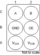
5 Pin Configuration and Functions
DBV, DCK, and DRL Package
6-Pin SOT-23, SC70, and SOT
Top View

Pin Functions
| PIN | TYPE | DESCRIPTION | ||
|---|---|---|---|---|
| NAME | DBV, DCK, DRL | YZP | ||
| A | 3 | C1 | I/O | Input/output A. Referenced to VCCA |
| B | 4 | C2 | I/O | Input/output B. Referenced to VCCB |
| GND | 2 | B1 | G | Ground |
| OE | 5 | B2 | I | Output enable. Pull OE low to place all outputs in 3-state mode. Referenced to VCCA. |
| VCCA | 1 | A1 | I | A-port supply voltage. 1.65 V ≤ VCCA ≤ 3.6 V and VCCA ≤ VCCB |
| VCCB | 6 | A2 | I | B-port supply voltage. 2.3 V ≤ VCCB ≤ 5.5 V |
