JAJSFE8K June 2006 – October 2023 TXS0104E
PRODUCTION DATA
- 1
- 1 特長
- 2 アプリケーション
- 3 概要
- 4 Revision History
- 5 Pin Configuration and Functions
-
6 Specifications
- 6.1 Absolute Maximum Ratings
- 6.2 ESD Ratings
- 6.3 Recommended Operating Conditions
- 6.4 Thermal Information: ZXU, YZT, and NMN
- 6.5 Thermal Information: D, PW, and RGY
- 6.6 Electrical Characteristics
- 6.7 Timing Requirements: VCCA = 1.8 V ± 0.15 V
- 6.8 Timing Requirements: VCCA = 2.5 V ± 0.2 V
- 6.9 Timing Requirements: VCCA = 3.3 V ± 0.3 V
- 6.10 Switching Characteristics: VCCA = 1.8 V ± 0.15 V
- 6.11 Switching Characteristics: VCCA = 2.5 V ± 0.2 V
- 6.12 Switching Characteristics: VCCA = 3.3 V ± 0.3 V
- 6.13 Typical Characteristics
- 7 Parameter Measurement Information
- 8 Detailed Description
- 9 Application and Implementation
- 10Device and Documentation Support
- 11Mechanical, Packaging, and Orderable Information
8.3.1 Architecture
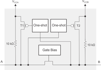
The TXS0104E architecture (see Figure 8-1) does not require a direction-control signal in order to control the direction of data flow from A to B or from B to A.
 Figure 8-1 Architecture of a TXS01xx Cell
Each A-port I/O has an internal 10-kΩ pullup resistor to VCCA, and each B-port I/O has an internal 10-kΩ pullup resistor to VCCB. The output one-shots detect rising edges on the A or B ports. During a rising edge, the one-shot turns on the PMOS transistors (T1, T2) for a short duration which speeds up the low-to-high transition.