JAJSHM6E june   2019  – february 2021 UCC256402 , UCC256403 , UCC256404

PRODUCTION DATA  

  1.   1
  2. 特長
  3. アプリケーション
  4. 概要
  5. Revision History
  6.   Device Comparison Table
  7. Pin Configuration and Functions
    1.     Pin Functions
  8. Specifications
    1. 6.1 Absolute Maximum Ratings
    2. 6.2 ESD Ratings
    3. 6.3 Recommended Operating Conditions
    4. 6.4 Thermal Information
    5. 6.5 Electrical Characteristics
    6. 6.6 Switching Characteristics
    7. 6.7 Typical Characteristics
  9. Detailed Description
    1. 7.1 Overview
    2. 7.2 Functional Block Diagram
    3. 7.3 Feature Description
      1. 7.3.1 Hybrid Hysteretic Control
      2. 7.3.2 Regulated 13-V Supply
      3. 7.3.3 Feedback Chain
        1. 7.3.3.1 Optocoupler Feedback Signal Input and Bias
        2. 7.3.3.2 FB Pin Voltage Clamp
        3. 7.3.3.3 "Pick Lower Value" Block and Soft Start Multiplexer
        4. 7.3.3.4 Pick Higher Block and Burst Mode Multiplexer
        5. 7.3.3.5 VCR Comparators
      4. 7.3.4 Resonant Capacitor Voltage Sensing
      5. 7.3.5 Resonant Current Sensing
      6. 7.3.6 Bulk Voltage Sensing
      7. 7.3.7 Output Voltage Sensing
      8. 7.3.8 High Voltage Gate Driver
        1. 7.3.8.1 Adaptive Dead Time Control
      9. 7.3.9 Protections
        1. 7.3.9.1 ZCS Region Prevention
        2. 7.3.9.2 Over Current Protection (OCP)
        3. 7.3.9.3 Bias Winding Over Voltage Protection (BWOVP)
        4. 7.3.9.4 Input Under Voltage Protection (VINUVP)
        5. 7.3.9.5 Input Over Voltage Protection (VINOVP)
        6. 7.3.9.6 Boot UVLO
        7. 7.3.9.7 RVCC UVLO
        8. 7.3.9.8 Over Temperature Protection (OTP)
    4. 7.4 Device Functional Modes
      1. 7.4.1 High Voltage Start-Up
      2. 7.4.2 X-Capacitor Discharge
      3. 7.4.3 Burst Mode Control
        1. 7.4.3.1 Soft-Start and Burst-Mode Threshold
        2. 7.4.3.2 BMTL/BMTH Ratio Programming
      4. 7.4.4 System State Machine
  10.   Application and Implementation
    1. 8.1 Application Information
    2. 8.2 Typical Application
      1. 8.2.1 Design Requirements
      2. 8.2.2 Detailed Design Procedure
        1. 8.2.2.1  LLC Power Stage Requirements
        2. 8.2.2.2  LLC Gain Range
        3. 8.2.2.3  Select Ln and Qe
        4. 8.2.2.4  Determine Equivalent Load Resistance
        5. 8.2.2.5  Determine Component Parameters for LLC Resonant Circuit
        6. 8.2.2.6  LLC Primary-Side Currents
        7. 8.2.2.7  LLC Secondary-Side Currents
        8. 8.2.2.8  LLC Transformer
        9. 8.2.2.9  LLC Resonant Inductor
        10. 8.2.2.10 LLC Resonant Capacitor
        11. 8.2.2.11 LLC Primary-Side MOSFETs
        12. 8.2.2.12 LLC Rectifier Diodes
        13. 8.2.2.13 LLC Output Capacitors
        14. 8.2.2.14 HV Pin Series Resistors
        15. 8.2.2.15 BLK Pin Voltage Divider
        16. 8.2.2.16 ISNS Pin Differentiator
        17. 8.2.2.17 VCR Pin Capacitor Divider
        18. 8.2.2.18 BW Pin Voltage Divider
        19. 8.2.2.19 Soft Start and Burst Mode Programming
      3. 8.2.3 Application Curves
  11. Power Supply Recommendations
    1. 8.1 VCC Pin Capacitor
    2. 8.2 Boot Capacitor
    3. 8.3 RVCC Pin Capacitor
  12. Layout
    1. 9.1 Layout Guidelines
    2. 9.2 Layout Example
  13. 10Device and Documentation Support
    1. 10.1 Documentation Support
      1. 10.1.1 Related Documentation
    2. 10.2 Related Links
    3. 10.3 Receiving Notification of Documentation Updates
    4. 10.4 Community Resources
    5. 10.5 Trademarks
  14.   Mechanical, Packaging, and Orderable Information

パッケージ・オプション

メカニカル・データ(パッケージ|ピン)
サーマルパッド・メカニカル・データ
発注情報

BLK Pin Voltage Divider

BLK pin senses the LLC input voltage and determines when to turn on and off the LLC converter. Different versions of UCC25640x have different BLK thresholds.

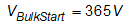
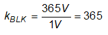
Choose bulk startup voltage at 365 V, then the BLK resistor divider ratio can be calculated as below:

Equation 44. GUID-894D3FAF-A826-481D-B413-FCB53FFD141B-low.gif

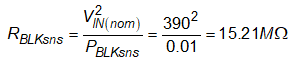
The desired power consumption of the BLK pin resistor divider is PBLKsns = 10 mW. The BLK sense resistor total value is given by:

Equation 45. GUID-00847B1E-BE98-43D3-810E-20E54768DAB2-low.gif

The lower BLK divider resistor value is given by:

Equation 46. GUID-DAC97465-2C39-4B19-9A97-F8D65283C47C-low.gif

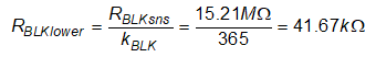
A standard value of 41.2 kΩ is selected for RBLKlower.The higher BLK divider resistor value is given by:

Equation 47. GUID-76A12065-4E40-4426-B22E-37DF78F38E8E-low.gif

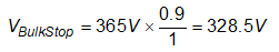
A standard value of 3x 4.99 MΩ in series is selected for RBLKupper. The actual bulk voltage thresholds can be calculated:

Equation 48. GUID-21CB3A37-2437-43F4-8F95-5AF0DC41EDEC-low.gif
Equation 49. GUID-1E2A6D29-B72E-466B-B655-9396FAD3EEE8-low.gif