JAJSHM6E june   2019  – february 2021 UCC256402 , UCC256403 , UCC256404

PRODUCTION DATA  

  1.   1
  2. 特長
  3. アプリケーション
  4. 概要
  5. Revision History
  6.   Device Comparison Table
  7. Pin Configuration and Functions
    1.     Pin Functions
  8. Specifications
    1. 6.1 Absolute Maximum Ratings
    2. 6.2 ESD Ratings
    3. 6.3 Recommended Operating Conditions
    4. 6.4 Thermal Information
    5. 6.5 Electrical Characteristics
    6. 6.6 Switching Characteristics
    7. 6.7 Typical Characteristics
  9. Detailed Description
    1. 7.1 Overview
    2. 7.2 Functional Block Diagram
    3. 7.3 Feature Description
      1. 7.3.1 Hybrid Hysteretic Control
      2. 7.3.2 Regulated 13-V Supply
      3. 7.3.3 Feedback Chain
        1. 7.3.3.1 Optocoupler Feedback Signal Input and Bias
        2. 7.3.3.2 FB Pin Voltage Clamp
        3. 7.3.3.3 "Pick Lower Value" Block and Soft Start Multiplexer
        4. 7.3.3.4 Pick Higher Block and Burst Mode Multiplexer
        5. 7.3.3.5 VCR Comparators
      4. 7.3.4 Resonant Capacitor Voltage Sensing
      5. 7.3.5 Resonant Current Sensing
      6. 7.3.6 Bulk Voltage Sensing
      7. 7.3.7 Output Voltage Sensing
      8. 7.3.8 High Voltage Gate Driver
        1. 7.3.8.1 Adaptive Dead Time Control
      9. 7.3.9 Protections
        1. 7.3.9.1 ZCS Region Prevention
        2. 7.3.9.2 Over Current Protection (OCP)
        3. 7.3.9.3 Bias Winding Over Voltage Protection (BWOVP)
        4. 7.3.9.4 Input Under Voltage Protection (VINUVP)
        5. 7.3.9.5 Input Over Voltage Protection (VINOVP)
        6. 7.3.9.6 Boot UVLO
        7. 7.3.9.7 RVCC UVLO
        8. 7.3.9.8 Over Temperature Protection (OTP)
    4. 7.4 Device Functional Modes
      1. 7.4.1 High Voltage Start-Up
      2. 7.4.2 X-Capacitor Discharge
      3. 7.4.3 Burst Mode Control
        1. 7.4.3.1 Soft-Start and Burst-Mode Threshold
        2. 7.4.3.2 BMTL/BMTH Ratio Programming
      4. 7.4.4 System State Machine
  10.   Application and Implementation
    1. 8.1 Application Information
    2. 8.2 Typical Application
      1. 8.2.1 Design Requirements
      2. 8.2.2 Detailed Design Procedure
        1. 8.2.2.1  LLC Power Stage Requirements
        2. 8.2.2.2  LLC Gain Range
        3. 8.2.2.3  Select Ln and Qe
        4. 8.2.2.4  Determine Equivalent Load Resistance
        5. 8.2.2.5  Determine Component Parameters for LLC Resonant Circuit
        6. 8.2.2.6  LLC Primary-Side Currents
        7. 8.2.2.7  LLC Secondary-Side Currents
        8. 8.2.2.8  LLC Transformer
        9. 8.2.2.9  LLC Resonant Inductor
        10. 8.2.2.10 LLC Resonant Capacitor
        11. 8.2.2.11 LLC Primary-Side MOSFETs
        12. 8.2.2.12 LLC Rectifier Diodes
        13. 8.2.2.13 LLC Output Capacitors
        14. 8.2.2.14 HV Pin Series Resistors
        15. 8.2.2.15 BLK Pin Voltage Divider
        16. 8.2.2.16 ISNS Pin Differentiator
        17. 8.2.2.17 VCR Pin Capacitor Divider
        18. 8.2.2.18 BW Pin Voltage Divider
        19. 8.2.2.19 Soft Start and Burst Mode Programming
      3. 8.2.3 Application Curves
  11. Power Supply Recommendations
    1. 8.1 VCC Pin Capacitor
    2. 8.2 Boot Capacitor
    3. 8.3 RVCC Pin Capacitor
  12. Layout
    1. 9.1 Layout Guidelines
    2. 9.2 Layout Example
  13. 10Device and Documentation Support
    1. 10.1 Documentation Support
      1. 10.1.1 Related Documentation
    2. 10.2 Related Links
    3. 10.3 Receiving Notification of Documentation Updates
    4. 10.4 Community Resources
    5. 10.5 Trademarks
  14.   Mechanical, Packaging, and Orderable Information

パッケージ・オプション

メカニカル・データ(パッケージ|ピン)
サーマルパッド・メカニカル・データ
発注情報

ISNS Pin Differentiator

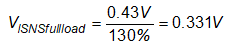
ISNS pin sets the over current protection level. OCP1 is peak current protection level; OCP2 and OCP3 are average current protection levels. The typical threshold voltages are 4.0 V, 0.6 V, and 0.43 V, respectively.

Set OCP3 level at 130% of full load. Thus, the sensed average input current level at full load is given by:

Equation 50. GUID-E206A77D-1A39-4ED3-9EC9-0B6A91BCA4E4-low.gif

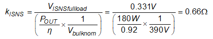
The current sense ratio can then be calculated:

Equation 51. GUID-0292E1BD-0F83-4023-B92F-7DACAB01827C-low.gif

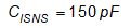
Select a current sense capacitor first, since there are less high voltage capacitor choices than resistors:

Equation 52. GUID-EE438B24-9D53-40B5-8985-9DF1DF29C75A-low.gif

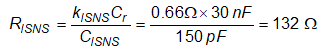
Then calculate the required ISNS resistor value:

Equation 53. GUID-A8F7E895-E289-4BDF-AFD5-9E6240614EAF-low.gif

After the current sense ratio is determined, the peak ISNS pin voltage at full load can be calculated:

Equation 54. GUID-EFA6DE2B-CE6A-4B7C-A4F5-200E7E22B4E0-low.gif

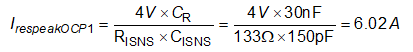
The peak resonant current at OCP1 level is given by:

Equation 55. GUID-8D34091D-A376-4AF0-8A25-D073654E6A9E-low.gif

The peak secondary-side current at OCP1 level is given by:

Equation 56. GUID-0F53770F-73D5-467A-8E2A-931F5AD1BECA-low.gif