JAJSC57F November 2002 – November 2023 UCC27423 , UCC27424 , UCC27425
PRODUCTION DATA
- 1
- 1 特長
- 2 アプリケーション
- 3 概要
- 4 Device Comparison Table
- 5 Pin Configuration and Functions
- 6 Specifications
- 7 Detailed Description
- 8 Application and Implementation
- 9 Power Supply Recommendations
- 10Layout
- 11Device and Documentation Support
- 12Revision History
- 13Mechanical, Packaging, and Orderable Information
パッケージ・オプション
デバイスごとのパッケージ図は、PDF版データシートをご参照ください。
メカニカル・データ(パッケージ|ピン)
- D|8
- P|8
- DGN|8
サーマルパッド・メカニカル・データ
- DGN|8
発注情報
8.2.2.2 Parallel Outputs
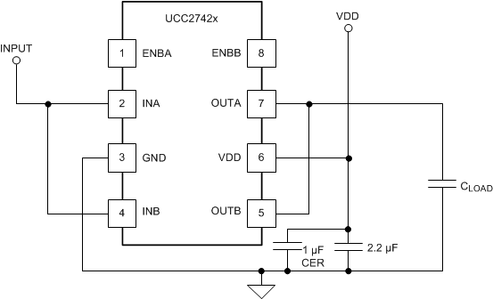
The A and B drivers may be combined into a single driver by connecting the INA and INB inputs together and the OUTA and OUTB outputs together. Then, a single signal can control the paralleled combination as shown in Figure 8-4.
 Figure 8-4 Parallel Operation of UCC27423 and UCC27424
Important consideration about paralleling two channels for UCC27423/4 include the INA and INB should be shorted in PCB layout as close to the device as possible, as well as for OUTA and OUTB, in which condition PCB layout parasitic mismatching between two channels could be minimized. The INA/B slope signal should be fast enough to avoid mismatched VIN_H / VIN_L, td1 / td2 between channel-A and channel-B. It is recommended to have input signal slope faster than 20 V/us.