JAJS127E April 1999 – August 2016 UCC2813-0 , UCC2813-1 , UCC2813-2 , UCC2813-3 , UCC2813-4 , UCC2813-5 , UCC3813-0 , UCC3813-1 , UCC3813-2 , UCC3813-3 , UCC3813-4 , UCC3813-5
PRODUCTION DATA.
- 1 特長
- 2 アプリケーション
- 3 概要
- 4 改訂履歴
- 5 Device Comparison Table
- 6 Pin Configuration and Functions
- 7 Specifications
-
8 Detailed Description
- 8.1 Overview
- 8.2 Functional Block Diagram
- 8.3
Feature Description
- 8.3.1 Detailed Pin Descriptions
- 8.3.2 Undervoltage Lockout (UVLO)
- 8.3.3 Self-Biasing, Active Low Output
- 8.3.4 Reference Voltage
- 8.3.5 Oscillator
- 8.3.6 Synchronization
- 8.3.7 PWM Generator
- 8.3.8 Minimum Off-Time Adjustment (Dead-Time Control)
- 8.3.9 Leading Edge Blanking
- 8.3.10 Minimum Pulse Width
- 8.3.11 Current Limiting
- 8.3.12 Overcurrent Protection and Full-Cycle Restart
- 8.3.13 Soft Start
- 8.3.14 Slope Compensation
- 8.4 Device Functional Modes
-
9 Application and Implementation
- 9.1 Application Information
- 9.2
Typical Application
- 9.2.1 Design Requirements
- 9.2.2
Detailed Design Procedure
- 9.2.2.1 Bulk Capacitor Calculation
- 9.2.2.2 Transformer Design
- 9.2.2.3 MOSFET and Output Diode Selection
- 9.2.2.4 Output Capacitor Calculation
- 9.2.2.5 Current Sensing Network
- 9.2.2.6 Gate Drive Resistor
- 9.2.2.7 REF Bypass Capacitor
- 9.2.2.8 RT and CT
- 9.2.2.9 Start-Up Circuit
- 9.2.2.10 Voltage Feedback Compensation Procedure
- 9.2.3 Application Curves
- 10Power Supply Recommendations
- 11Layout
- 12デバイスおよびドキュメントのサポート
- 13メカニカル、パッケージ、および注文情報
パッケージ・オプション
デバイスごとのパッケージ図は、PDF版データシートをご参照ください。
メカニカル・データ(パッケージ|ピン)
- D|8
- PW|8
サーマルパッド・メカニカル・データ
発注情報
7 Specifications
7.1 Absolute Maximum Ratings
over operating free-air temperature range (unless otherwise noted)(1)(2)| MIN | MAX | UNIT | ||
|---|---|---|---|---|
| VCC voltage(3) | 12 | V | ||
| VCC current | 30 | mA | ||
| OUT current | ±1 | A | ||
| OUT energy (capacitive load) | 20 | µJ | ||
| Analog inputs | FB, CS, RC, COMP | –0.3 | 6.3 or VVCC + 0.3(4) |
V |
| Power dissipation at TA < 25°C | N package | 1 | W | |
| D package | 0.65 | |||
| Lead temperature, soldering (10 s) | 300 | °C | ||
| Junction temperature | –55 | 150 | °C | |
| Storage temperature, Tstg | –65 | 150 | °C | |
(1) All voltages are with respect to GND. All currents are positive into the specified terminal.
(2) Stresses beyond those listed under Absolute Maximum Ratings may cause permanent damage to the device. These are stress ratings only, which do not imply functional operation of the device at these or any other conditions beyond those indicated under Recommended Operating Conditions. Exposure to absolute-maximum-rated conditions for extended periods may affect device reliability.
(3) In normal operation VCC is powered through a current limiting resistor. The resistor must be sized so that the VCC voltage under operating conditions is below 12 V but above the turnoff threshold. Absolute maximum of 12 V applies when VCC is driven from a low impedance source such that ICC does not exceed 30 mA.
(4) Whichever is smaller.
7.2 ESD Ratings
| VALUE | UNIT | |||
|---|---|---|---|---|
| V(ESD) | Electrostatic discharge | Human-body model (HBM), per ANSI/ESDA/JEDEC JS-001(1) | ±2500 | V |
| Charged-device model (CDM), per JEDEC specification JESD22-C101(2) | ±1500 | |||
(1) JEDEC document JEP155 states that 500-V HBM allows safe manufacturing with a standard ESD control process.
(2) JEDEC document JEP157 states that 250-V CDM allows safe manufacturing with a standard ESD control process.
7.3 Recommended Operating Conditions
over operating free-air temperature range (unless otherwise noted)| MIN | MAX | UNIT | |||
|---|---|---|---|---|---|
| VVCC | VCC bias supply voltage from a low impedance source | 11 | V | ||
| IVCC | Supply bias current | 25 | mA | ||
| VOUT | Gate driver output voltage | –0.1 | VVCC | V | |
| IOUT | Average OUT pin current | 20 | mA | ||
| IREF | REF pin output current | 5 | mA | ||
| Voltage on analog pins | FB, CS, RC, COMP | –0.1 | 6 or VVCC(1) | V | |
| fOSC | Oscillator frequency | 1 | MHz | ||
(1) Whichever is smaller.
7.4 Thermal Information
| THERMAL METRIC(1) | UCCx813-x | UNIT | |||
|---|---|---|---|---|---|
| P (PDIP) | D (SOIC) | PW (TSSOP) | |||
| 8 PINS | 8 PINS | 8 PINS | |||
| RθJA | Junction-to-ambient thermal resistance | 50.9 | 107.5 | 153.8 | °C/W |
| RθJC(top) | Junction-to-case (top) thermal resistance | 40.3 | 49.3 | 38.4 | °C/W |
| RθJB | Junction-to-board thermal resistance | 28.1 | 48.7 | 83.8 | °C/W |
| ψJT | Junction-to-top characterization parameter | 17.6 | 6.6 | 2.2 | °C/W |
| ψJB | Junction-to-board characterization parameter | 28 | 48 | 82 | °C/W |
(1) For more information about traditional and new thermal metrics, see the Semiconductor and IC Package Thermal Metrics application report.
7.5 Electrical Characteristics
Unless otherwise stated, these specifications apply for –40°C ≤ TA ≤ 85°C for the UCC2813-x device; 0°C ≤ TA ≤ 70°C for the UCC3813-x device, TJ = TA; VVCC = 10 V(1); RT = 100 kΩ from REF to RC; CT = 330 pF from RC to GND; 0.1-µF capacitor from VCC to GND; 0.1-µF capacitor from VREF to GND.| PARAMETER | TEST CONDITIONS | MIN | TYP | MAX | UNIT | |
|---|---|---|---|---|---|---|
| REFERENCE | ||||||
| Output voltage | TJ = 25°C, I = 0.2 mA, UCCx813-[0,1,2,4] | 4.925 | 5 | 5.075 | V | |
| TJ = 25°C, I = 0.2 mA, UCCx813-[3,5] | 3.94 | 4 | 4.06 | |||
| Load regulation | 0.2 mA < I < 5 mA | 10 | 30 | mV | ||
| Total variation | UCCx813-[0,1,2,4](5) | 4.84 | 5 | 5.1 | V | |
| UCCx813-[3,5](5) | 3.84 | 4 | 4.08 | |||
| Output noise voltage | 10 Hz ≤ f ≤ 10 kHz, TJ = 25°C(7) | 70 | µV | |||
| Long term stability | TA = 125°C, 1000 hours(7) | 5 | mV | |||
| Output short circuit | –5 | –35 | mA | |||
| OSCILLATOR | ||||||
| Oscillator frequency | UCCx813-[0,1,2,4](2) | 40 | 46 | 52 | kHz | |
| UCCx813-[3,5](2) | 26 | 31 | 36 | |||
| Temperature stability | See note (7) | 2.5% | ||||
| Amplitude peak-to-peak | 2.25 | 2.4 | 2.55 | V | ||
| Oscillator peak voltage | 2.45 | V | ||||
| ERROR AMPLIFIER | ||||||
| Input voltage | VCOMP = 2.5 V; UCCx813-[0,1,2,4] | 2.42 | 2.5 | 2.56 | V | |
| VCOMP = 2 V; UCCx813-[3,5] | 1.92 | 2 | 2.05 | |||
| Input bias current | –2 | 2 | µA | |||
| Open loop voltage gain | 60 | 80 | dB | |||
| COMP sink current | VFB = 2.7 V, VCOMP = 1.1 V | 0.4 | 2.5 | mA | ||
| COMP source current | VFB = 1.8 V, VCOMP = VREF – 1.2 V | –0.2 | –0.5 | –0.8 | mA | |
| Gain-bandwidth product | See note (7) | 2 | MHz | |||
| PWM | ||||||
| Maximum duty cycle | UCCx813-[0,2,3] | 97% | 99% | 100% | ||
| UCCx813-[1,4,5] | 48% | 49% | 50% | |||
| Minimum duty cycle | VCOMP = 0 V | 0% | ||||
| CURRENT SENSE | ||||||
| Gain | See note (3) | 1.1 | 1.65 | 1.8 | V/V | |
| Maximum input signal | VCOMP = 5 V(4) | 0.9 | 1 | 1.1 | V | |
| Input bias current | –200 | 200 | nA | |||
| CS blank time | 50 | 100 | 150 | ns | ||
| Overcurrent threshold | 1.32 | 1.55 | 1.7 | V | ||
| COMP to CS offset | VCS = 0 V | 0.45 | 0.9 | 1.35 | V | |
| OUTPUT | ||||||
| OUT low level | I = 20 mA, all parts | 0.1 | 0.4 | V | ||
| I = 200 mA, all parts | 0.35 | 0.9 | ||||
| I = 50 mA, VVCC = 5 V, UCCx813-[3,5] | 0.15 | 0.4 | ||||
| I = 20 mA, VCC = 0 V, all parts | 0.7 | 1.2 | ||||
| VVCC – OUT | OUT high Vsat | I = –20 mA, all parts | 0.15 | 0.4 | V | |
| I = –200 mA, all parts | 1 | 1.9 | ||||
| I = –50 mA, VVCC = 5 V, UCCx813-[3,5] | 0.4 | 0.9 | ||||
| Rise time | CL = 1 nF | 41 | 70 | ns | ||
| Fall time | CL = 1 nF | 44 | 75 | ns | ||
| UNDERVOLTAGE LOCKOUT | ||||||
| Start threshold (6) | UCCx813-0 | 6.6 | 7.2 | 7.8 | V | |
| UCCx813-1 | 8.6 | 9.4 | 10.2 | |||
| UCCx813-[2,4] | 11.5 | 12.5 | 13.5 | |||
| UCCx813-[3,5] | 3.7 | 4.1 | 4.5 | |||
| Stop threshold (6) | UCCx813-0 | 6.3 | 6.9 | 7.5 | V | |
| UCCx813-1 | 6.8 | 7.4 | 8 | |||
| UCCx813-[2,4] | 7.6 | 8.3 | 9 | |||
| UCCx813-[3,5] | 3.2 | 3.6 | 4 | |||
| Start to stop hysteresis | UCCx813-0 | 0.12 | 0.3 | 0.48 | V | |
| UCCx813-1 | 1.6 | 2 | 2.4 | |||
| UCCx813-[2,4] | 3.5 | 4.2 | 5.1 | |||
| UCCx813-[3,5] | 0.2 | 0.5 | 0.8 | |||
| SOFT START | ||||||
| COMP rise time | VFB = 1.8 V, Rise from 0.5 V to REF – 1 V | 4 | ms | |||
| OVERALL | ||||||
| Start-up current | VVCC < start threshold | 0.1 | 0.23 | mA | ||
| Operating supply current | VFB = 0 V, VCS = 0 V, VRC = 0 V | 0.5 | 1.2 | mA | ||
| VCC internal Zener voltage(6) | ICC = 10 mA | 12 | 13.5 | 15 | V | |
| VCC internal Zener voltage minus start-threshold voltage (6) | UCCx813-[2,4] | 0.5 | 1 | V | ||
(1) Adjust VCC above the start threshold before setting at 10 V.
(2) Output frequency for the UCCx813-[0,2,3] device is the oscillator frequency. Output frequency for the UCCx813-[1,4,5] device is one-half the oscillator frequency.
(3) Gain is defined by:  .
.
 .
.(4) Parameter measured at trip point of latch with FB at 0 V.
(5) Total variation includes temperature stability and load regulation.
(6) Start threshold, stop threshold, and Zener-shunt thresholds track one another.
(7) Ensured by design. Not 100% tested in production.
7.6 Typical Characteristics
![UCC2813-0 UCC2813-1 UCC2813-2 UCC2813-3 UCC2813-4 UCC2813-5 UCC3813-0 UCC3813-1 UCC3813-2 UCC3813-3 UCC3813-4 UCC3813-5 UCC3813-[0,1,2,4]:
Oscillator Frequency vs
RT and CT UCC2813-0 UCC2813-1 UCC2813-2 UCC2813-3 UCC2813-4 UCC2813-5 UCC3813-0 UCC3813-1 UCC3813-2 UCC3813-3 UCC3813-4 UCC3813-5 13_1_2_4_osc_freq_SLUS161.gif](/ods/images/JAJS127E/13_1_2_4_osc_freq_SLUS161.gif) Figure 3. UCC3813-[0,1,2,4]: Oscillator Frequency vs
Figure 3. UCC3813-[0,1,2,4]: Oscillator Frequency vsRT and CT
![UCC2813-0 UCC2813-1 UCC2813-2 UCC2813-3 UCC2813-4 UCC2813-5 UCC3813-0 UCC3813-1 UCC3813-2 UCC3813-3 UCC3813-4 UCC3813-5 UCC3813-[0,2,3]: Maximum
Duty Cycle vs
Oscillator Frequency UCC2813-0 UCC2813-1 UCC2813-2 UCC2813-3 UCC2813-4 UCC2813-5 UCC3813-0 UCC3813-1 UCC3813-2 UCC3813-3 UCC3813-4 UCC3813-5 2_3_max_duty_cyc_SLUS161.gif](/ods/images/JAJS127E/2_3_max_duty_cyc_SLUS161.gif) Figure 5. UCC3813-[0,2,3]: Maximum Duty Cycle vs
Figure 5. UCC3813-[0,2,3]: Maximum Duty Cycle vsOscillator Frequency
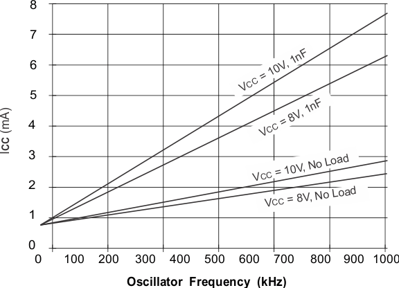
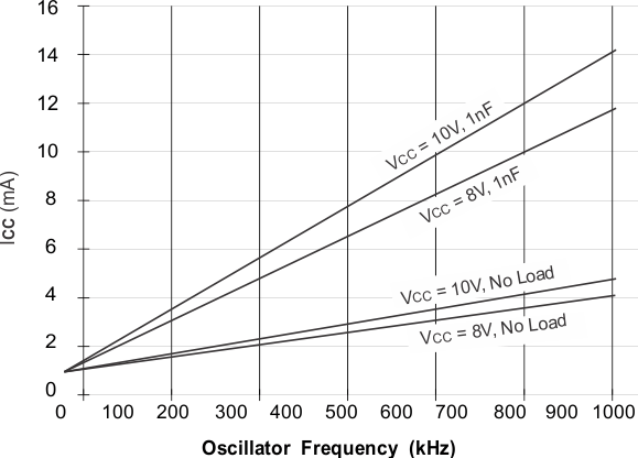 Figure 7. UCC3813-0: ICC vs Oscillator Frequency
![UCC2813-0 UCC2813-1 UCC2813-2 UCC2813-3 UCC2813-4 UCC2813-5 UCC3813-0 UCC3813-1 UCC3813-2 UCC3813-3 UCC3813-4 UCC3813-5 UCC3813-[3,5]:
VREF vs VCC UCC2813-0 UCC2813-1 UCC2813-2 UCC2813-3 UCC2813-4 UCC2813-5 UCC3813-0 UCC3813-1 UCC3813-2 UCC3813-3 UCC3813-4 UCC3813-5 VREF_vs_VCC_SLUS161.gif](/ods/images/JAJS127E/VREF_vs_VCC_SLUS161.gif)
![UCC2813-0 UCC2813-1 UCC2813-2 UCC2813-3 UCC2813-4 UCC2813-5 UCC3813-0 UCC3813-1 UCC3813-2 UCC3813-3 UCC3813-4 UCC3813-5 UCC3813-[3,5]:
Oscillator Frequency vs RT and CT UCC2813-0 UCC2813-1 UCC2813-2 UCC2813-3 UCC2813-4 UCC2813-5 UCC3813-0 UCC3813-1 UCC3813-2 UCC3813-3 UCC3813-4 UCC3813-5 13_3_5_osc_freq_SLUS161.gif](/ods/images/JAJS127E/13_3_5_osc_freq_SLUS161.gif)
![UCC2813-0 UCC2813-1 UCC2813-2 UCC2813-3 UCC2813-4 UCC2813-5 UCC3813-0 UCC3813-1 UCC3813-2 UCC3813-3 UCC3813-4 UCC3813-5 UCC3813-[1,4,5]: Maximum
Duty Cycle vs
Oscillator Frequency UCC2813-0 UCC2813-1 UCC2813-2 UCC2813-3 UCC2813-4 UCC2813-5 UCC3813-0 UCC3813-1 UCC3813-2 UCC3813-3 UCC3813-4 UCC3813-5 4_5_max_duty_cyc_SLUS161.gif](/ods/images/JAJS127E/4_5_max_duty_cyc_SLUS161.gif)
