JAJS365D January 2007 – October 2019 TPS2412 , TPS2413
PRODUCTION DATA.
- 1 特長
- 2 アプリケーション
- 3 概要
- 4 改訂履歴
- 5 概要(続き)
- 6 Device Comparison Table
- 7 Pin Configuration and Functions
- 8 Specifications
-
9 Detailed Description
- 9.1 Overview
- 9.2 Functional Block Diagram
- 9.3
Feature Description
- 9.3.1 Definitions
- 9.3.2 TPS2412 vs TPS2413 – MOSFET Control Methods
- 9.3.3 N+1 Power Supply – Typical Connection
- 9.3.4 Input ORing – Typical Connection
- 9.3.5 System Design and Behavior With Transients
- 9.3.6 TPS2412 Regulation-Loop Stability
- 9.3.7 MOSFET Selection and R(RSET)
- 9.3.8 Gate Drive, Charge Pump and C(BYP)
- 9.4 Device Functional Modes
- 10Application and Implementation
- 11Power Supply Recommendations
- 12Layout
- 13デバイスおよびドキュメントのサポート
- 14メカニカル、パッケージ、および注文情報
10.2 Typical Application
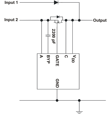
Applications with the TPS2412/13 are not limited to ORing of identical sections. The TPS2412/13 and external MOSFET form a general purpose function block. Figure 11 shows a circuit with ORing between a discrete diode and a TPS2412/MOSFET section. This circuit can be used to combine two different voltages in cases where the output is regulated, and the additional voltage drop in the Input 1 path is not a concern. An example is ORing of an AC adapter on Input 1 with a lower voltage on Input 2.
 Figure 11. ORing Circuit
 The TPS2412 may be a better choice in applications where inputs may be removed, causing an open-circuit input. If the MOSFET was ON when the input is removed, VAC will be virtually zero. If the reverse turnoff threshold is programmed negative, the TPS2412/13 will not pull GATE low. A system interruption could then be created if a short is applied to the floating input. For example, if an AC adapter is first connected to the unit, and then connected to the AC mains, the adapter's output capacitors will look like a momentary short to the unit. A TPS2412 with RSET open will turn the MOSFET OFF when the input goes open circuit.