JAJS472C August 2010 – April 2018 TPS54320
PRODUCTION DATA.
- 1 特長
- 2 アプリケーション
- 3 概要
- 4 改訂履歴
- 5 Pin Configuration and Functions
- 6 Specifications
-
7 Detailed Description
- 7.1 Overview
- 7.2 Functional Block Diagram
- 7.3
Feature Description
- 7.3.1 Fixed Frequency PWM Control
- 7.3.2 Continuous Current Mode Operation (CCM)
- 7.3.3 VIN and Power VIN Pins (VIN and PVIN)
- 7.3.4 Voltage Reference
- 7.3.5 Adjusting the Output Voltage
- 7.3.6 Safe Start-up into Prebiased Outputs
- 7.3.7 Error Amplifier
- 7.3.8 Slope Compensation
- 7.3.9 Enable and Adjusting UVLO
- 7.3.10 Slow Start (SS/TR)
- 7.3.11 Power Good (PWRGD)
- 7.3.12 Bootstrap Voltage (BOOT) and Low Dropout Operation
- 7.3.13 Sequencing (SS/TR)
- 7.3.14 Output Overvoltage Protection (OVP)
- 7.3.15 Overcurrent Protection
- 7.3.16 Thermal Shutdown
- 7.3.17 Small Signal Model for Loop Response
- 7.3.18 Simple Small Signal Model for Peak Current Mode Control
- 7.3.19 Small Signal Model for Frequency Compensation
- 7.4 Device Functional Modes
-
8 Application and Implementation
- 8.1 Application Information
- 8.2
Typical Application
- 8.2.1 Design Requirements
- 8.2.2
Detailed Design Procedure
- 8.2.2.1 Custom Design With WEBENCH® Tools
- 8.2.2.2 Operating Frequency
- 8.2.2.3 Output Inductor Selection
- 8.2.2.4 Output Capacitor Selection
- 8.2.2.5 Input Capacitor Selection
- 8.2.2.6 Slow-Start Capacitor Selection
- 8.2.2.7 Bootstrap Capacitor Selection
- 8.2.2.8 UVLO Set Point
- 8.2.2.9 Output Voltage Feedback Resistor Selection
- 8.2.2.10 Compensation Component Selection
- 8.2.3 Application Curves
- 9 Power Supply Recommendations
- 10Layout
- 11デバイスおよびドキュメントのサポート
- 12メカニカル、パッケージ、および注文情報
7.4.3 Synchronization (CLK Mode)
An internal PLL has been implemented to allow synchronization between 200 kHz and 1.2 MHz, and to easily switch from RT mode to CLK mode.
To implement the synchronization feature, connect a square wave clock signal to the RT/CLK pin with a duty cycle between 20% to 80%. The clock signal amplitude must transition lower than 0.8 V and higher than 2.0 V. The start of the switching cycle is synchronized to the falling edge of RT/CLK pin.
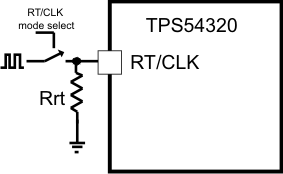
In applications where both RT mode and CLK mode are needed, the device can be configured as shown in Figure 33. Before the external clock is present, the device works in RT mode and the switching frequency is set by RT resistor. When the external clock is present, the CLK mode overrides the RT mode. The first time the RT/CLK pin is pulled above the RT/CLK high threshold (2.0 V), the device switches from the RT mode to the CLK mode and the RT/CLK pin becomes high impedance as the PLL starts to lock onto the frequency of the external clock. TI does not recommend to switch from the CLK mode back to the RT mode, because the internal switching frequency drops to 100 kHz first before returning to the switching frequency set by RT resistor.
 Figure 33. Works With Both RT Mode and CLK Mode