JAJSC03E january   2014  – may 2023 TPS562200 , TPS563200

PRODUCTION DATA  

  1.   1
  2. 特長
  3. アプリケーション
  4. 概要
  5. Revision History
  6. Pin Configuration and Functions
  7. Specifications
    1. 6.1 Absolute Maximum Ratings #GUID-10807E29-2FD4-4A3F-94B2-FDEBD147A133/SLVSC819633
    2. 6.2 ESD Ratings
    3. 6.3 Recommended Operating Conditions
    4. 6.4 Thermal Information
    5. 6.5 Electrical Characteristics
    6. 6.6 Timing Requirements
    7. 6.7 Typical Characteristics TPS562200
    8. 6.8 Typical Characteristics TPS563200
  8. Detailed Description
    1. 7.1 Overview
    2. 7.2 Functional Block Diagram
    3. 7.3 Feature Description
      1. 7.3.1 The Adaptive On-Time Control And PWM Operation
      2. 7.3.2 Advanced Eco-mode Control
      3. 7.3.3 Soft Start And Pre-Biased Soft Start
      4. 7.3.4 Current Protection
      5. 7.3.5 Over Voltage Protection
      6. 7.3.6 UVLO Protection
      7. 7.3.7 Thermal Shutdown
    4. 7.4 Device Functional Modes
      1. 7.4.1 Normal Operation
      2. 7.4.2 Eco-mode Operation
      3. 7.4.3 Standby Operation
  9. Application and Implementation
    1. 8.1 Application Information
    2. 8.2 Typical Applications
      1. 8.2.1 Tps562200 4.5-V To 17-V Input, 1.05-V Output Converter
        1. 8.2.1.1 Design Requirements
        2. 8.2.1.2 Detailed Design Procedures
          1. 8.2.1.2.1 Custom Design with WEBENCH® Tools
          2. 8.2.1.2.2 Output Voltage Resistors Selection
          3. 8.2.1.2.3 Output Filter Selection
          4. 8.2.1.2.4 Input Capacitor Selection
          5. 8.2.1.2.5 Bootstrap Capacitor Selection
        3. 8.2.1.3 Application Curves
      2. 8.2.2 Tps563200 4.5-V To 17-V Input, 1.05-V Output Converter
        1. 8.2.2.1 Design Requirements
        2. 8.2.2.2 Detailed Design Procedures
          1. 8.2.2.2.1 Output Filter Selection
        3. 8.2.2.3 Application Curves
    3. 8.3 Power Supply Recommendations
    4. 8.4 Layout
      1. 8.4.1 Layout Guidelines
      2. 8.4.2 Layout Example
  10. Device and Documentation Support
    1. 9.1 Device Support
      1. 9.1.1 Development Support
        1. 9.1.1.1 Custom Design with WEBENCH® Tools
    2. 9.2 ドキュメントの更新通知を受け取る方法
    3. 9.3 サポート・リソース
    4. 9.4 Trademarks
    5. 9.5 静電気放電に関する注意事項
    6. 9.6 用語集
  11. 10Mechanical, Packaging, And Orderable Information

Application Curves

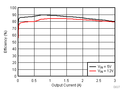
GUID-2EFC03B4-3F56-4BFC-B9B9-473687500321-low.gifFigure 8-17 Tps563200 Efficiency
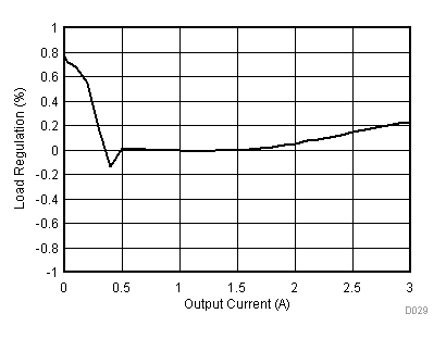
GUID-C923D752-BA1F-4E37-B62C-7AAED84891A1-low.gifFigure 8-19 Tps563200 Load Regulation, VI = 5 V
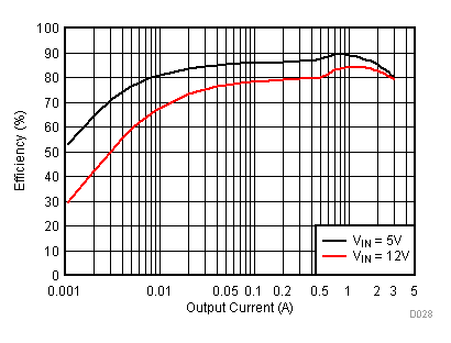
GUID-BCF378F7-0EA8-4FEA-9BF2-1AF5D2798F10-low.gifFigure 8-18 Tps563200 Light Load Efficiency
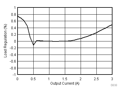
GUID-01D3B15F-B1FF-484C-945F-6E84C93A5804-low.gifFigure 8-20 Tps563200 Load Regulation, VI = 12 V
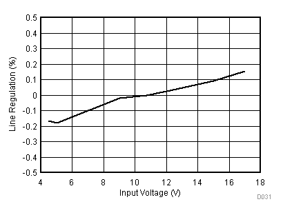
GUID-350560E8-9A92-4926-831E-A888A31318A7-low.gifFigure 8-21 Tps563200 Line Regulation
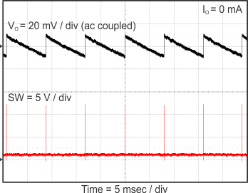
GUID-BA84AB5D-DA68-4EEA-8440-0609756D540F-low.gifFigure 8-23 Tps563200 Output Voltage Ripple
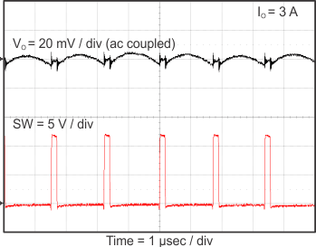
GUID-548FED63-E519-4B09-BB1C-65D4874E128C-low.gifFigure 8-25 Tps563200 Output Voltage Ripple
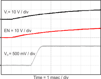
GUID-097E356D-09F5-48AD-A013-570C0B28C885-low.gifFigure 8-27 Tps563200 Start-up Relative to VI
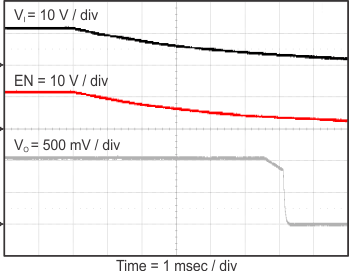
GUID-D3DA7CFB-4601-4882-99BF-F770AB341CF2-low.gifFigure 8-29 Tps563200 Shut Down Relative to VI
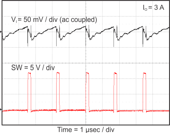
GUID-6BB672DD-41F2-49F7-9D50-4222FC4CC832-low.gifFigure 8-22 Tps563200 Input Voltage Ripple
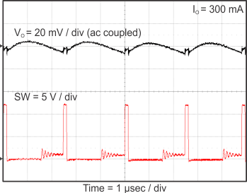
GUID-5C1C51B7-F9CA-4C63-82FD-CDE003AC0AC3-low.gifFigure 8-24 Tps563200 Output Voltage Ripple
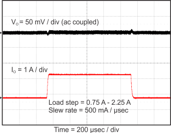
GUID-AD88CCFF-0EAE-494B-AA80-B820B0558B83-low.gifFigure 8-26 Tps563200 Transient Response
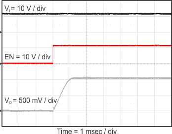
GUID-EA4D51A0-62BD-4A23-921E-21128737EBB8-low.gifFigure 8-28 Tps563200 Start-up Relative to En
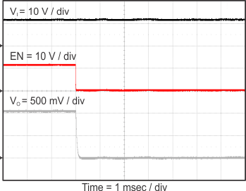
GUID-439AFC36-4E6B-4ECC-830F-A3B1E01A4797-low.gifFigure 8-30 Tps563200 Shutdown Relative to En